Erasing device for liquid crystal display image and liquid crystal display device including the same

a liquid crystal display and image technology, applied in the field of liquid crystal display image and liquid crystal display device including the same, can solve the problems of vivid display errors, degraded image quality of this kind, and degraded display quality, so as to suppress the deterioration of liquid crystal and quickly erase the afterimage

Inactive Publication Date: 2006-01-12
SHARP KK
View PDF0 Cites 16 Cited by
  • Summary
  • Abstract
  • Description
  • Claims
  • Application Information

AI Technical Summary

Benefits of technology

[0015] It is therefore an object of the present invention to provide an erasing device for a liquid crystal display image which can erase an afterimage quickly while suppressing the deterioration of the liquid crystal, and to provide a liquid crystal displace device including such an erasing device.
[0021] Thus, the OFF signal that turns OFF the power source of the main body of the liquid crystal display device can be a signal based on a command to turn OFF the liquid crystal display device or a signal indicating the disconnection of the power source for some reason. Upon detection of the OFF signal, the power source OFF detecting section conveys the detection result to both the panel power maintaining section and erasing section. Accordingly, the panel power maintaining section supplies power to the liquid crystal display panel for a certain period, so that the liquid crystal display panel can keep displaying an image after the power source of the main body of the liquid crystal display device is turned OFF. Consequently, it has become possible to drive the liquid crystal display panel after the power source of the main body of the liquid crystal display device is turned OFF.
[0023] Accordingly, even if a half-tone image is displayed on the liquid crystal display panel before the power source of the main body of the liquid crystal display device is turned OFF and an amount of the restoring energy of the liquid crystal is small because the distortion is minor, the saturation voltage is applied to the liquid crystal of the liquid crystal display panel to increase an amount of the restoring energy to a satisfactory level. Thus, when the liquid crystal display panel is shut off entirely after being lit up entirely, the liquid crystal is turned OFF quickly. In other words, an afterimage on the liquid crystal display panel can be erased quickly.
[0024] In this case, an afterimage can be erased faster if the liquid crystal display panel is arranged to apply a voltage which turns OFF the liquid crystal to the liquid crystal when lighting up and subsequently shutting off the liquid crystal display panel entirely.
[0026] If the TFTs (Thin Film Transistors) are used as the active elements, liquid crystal with high maintaining ability is required, and in general, liquid crystal with high specific resistance (1×10¹²Ω·cm) is used. It takes a long time for the liquid crystal with high specific resistance to discharge the charges, and it is more difficult to erase an afterimage. However, applying the saturation voltage before applying a voltage which turns OFF the liquid crystal in the above manner is very effective in such a case.
[0027] If an afterimage on the liquid crystal display panel is erased quickly, the charges withheld in the liquid crystal are discharged in a short time, thereby making it possible to suppress the deterioration of the liquid crystal due to an abnormal voltage.

Problems solved by technology

The afterimage degrades the image quality of this kind of liquid crystal display device serving as a display machine.
However, since the reflective liquid crystal display device can not block the incident light, it is impossible to make the afterimage less noticeable, thereby showing a display error vividly.
Further, the charges withheld in the liquid crystal due to an abnormal voltage not only degrade the display quality by the afterimage, but also give adverse effects on the operation life of the liquid crystal.
This is because, when a voltage around the threshold voltage is applied to the liquid crystal, the distortion of the liquid crystal is so minor that only a small amount of energy is required to restore the liquid crystal.
If such an afterimage is erased by the method disclosed in aforementioned Japanese Laid-open Patent Application No. 170986 (Tokukaihei 1-170986), that is, by releasing the charges withheld in the liquid crystal by maintaining the gate at an active level for a certain period after the power source is turned OFF, it takes a long time to release all the charges, thereby making it impossible to erase the afterimage quickly.
Thus, in practice, a residual voltage is applied to the liquid crystal, and the above method presumably can not attain a desired afterimage erasing effect.
If the transmission liquid crystal display device adopts the above erasing method, still the afterimage appears after the power source is turned OFF; although the afterimage appears slightly for a short period, it is enough to degrade the image quality.
Also, if it takes a long time to erase the afterimage, an abnormal voltage is applied to the liquid crystal due to the charges withheld therein even for a short period, and as a consequence, the liquid crystal deteriorates.
Thus, the liquid crystal deteriorates more or less the same extent in both the reflective and transmission liquid crystal display devices, but the display quality is deteriorated far worse in the reflective liquid crystal display device than in the transmission type.

Method used


Image

  • Erasing device for liquid crystal display image and liquid crystal display device including the same
  • Erasing device for liquid crystal display image and liquid crystal display device including the same
  • Erasing device for liquid crystal display image and liquid crystal display device including the same

Examples


first embodiment

[0062] The following description will describe a first embodiment of the present invention.

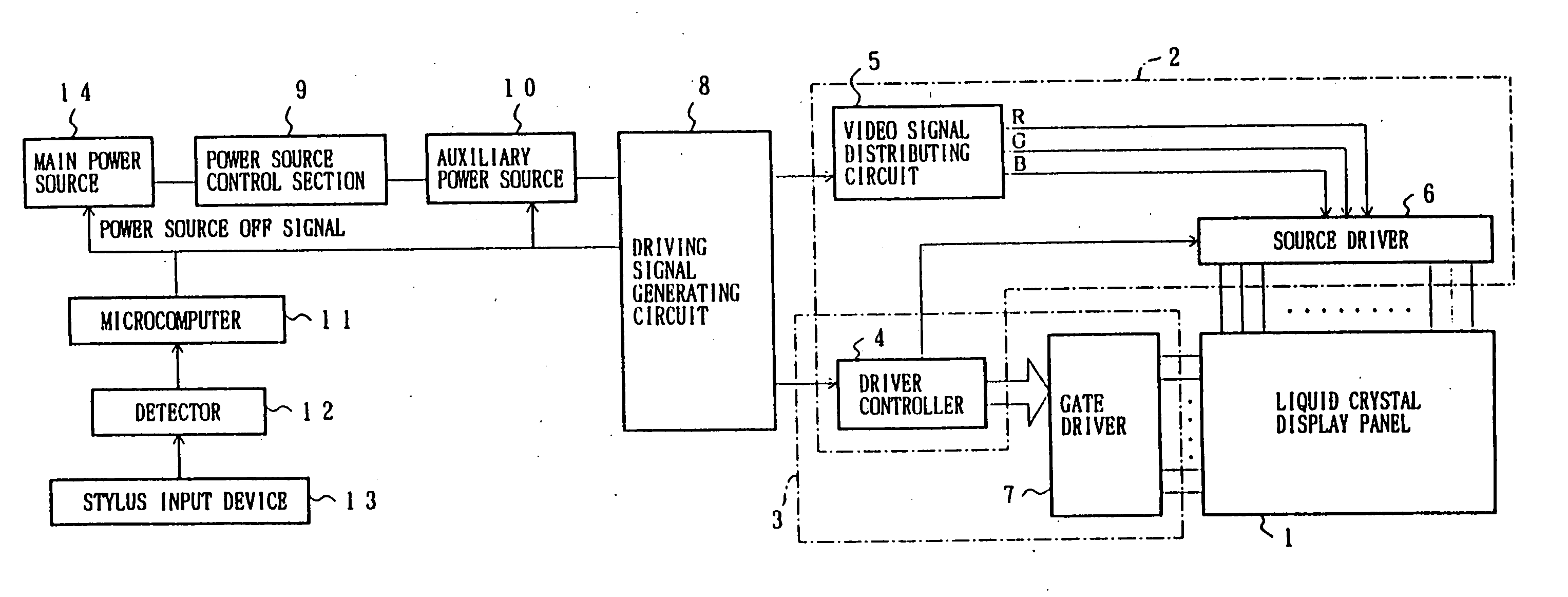
[0063]FIG. 1 is a block diagram depicting an arrangement of a liquid crystal display device id accordance with the present embodiment (hereinafter, referred to as the present liquid crystal display device). As shown in the drawing, the present liquid crystal display device includes a liquid crystal display panel 1, a source driving section 2, a gate driving section 3, a driving signal generating circuit 8, a power source control section 9, an auxiliary power source 10, a microcomputer 11, a detector 12, a stylus input device 13, and a main power source 14.

[0064] The liquid crystal display panel 1 comprises a pair of glass substrates laminated to each other, and GH (Guest-Host) liquid crystal sandwiched by the substrates. The liquid crystal display panel 1 further comprises a reflector, and serves as a reflective liquid crystal display panel which displays an image using incident light from t...

second embodiment

[0083] The following description will describe a second embodiment of the present invention. Hereinafter, like components are labeled with like reference numerals with respect to the first embodiment, and the description of these components is not repeated for the explanation's convenience.

[0084]FIG. 4 is a block diagram depicting an arrangement of a liquid crystal display device in accordance with the present embodiment (hereinafter, referred to as the present liquid crystal display device). As shown in the drawing, the present liquid crystal display device includes a source side compensating circuit 31 between a driving signal generating circuit 8′ and the video signal distributing circuit 5, and a gate side compensating circuit 30 between a driver controller 4′ and the gate driver 7.

[0085] The driving signal generating circuit 8′ outputs an ON-level composite video signal which lights up the liquid crystal display panel 1 entirely on the saturation voltage of the liquid crystal...

third embodiment

[0101] The following description will describe a third embodiment of the present invention, Hereinafter, like components are labeled with like reference numerals with respect to the above embodiments, and the description of these components is not repeated for the explanation's convenience.

[0102]FIG. 10 is a block diagram depicting a liquid crystal display device in accordance with the present embodiment (hereinafter, referred to as the present liquid crystal display device). As shown in the drawing, the source side compensating circuit 31 is provided between the driving signal generating circuit 8′ and video signal distributing circuit 5. Also, a driver controller 35 provided herein latches and withholds the vertical synchronizing signals, and upon input of the power source OFF signal, the driver controller 35 extends all the withheld vertical synchronizing signals concurrently for a certain period and outputs the resulting signals.

[0103] In the present liquid crystal display dev...


PUM

PropertyMeasurementUnit
voltageaaaaaaaaaa
applied voltageaaaaaaaaaa
poweraaaaaaaaaa

Abstract

An erasing device for a liquid crystal display image of the present invention is furnished with an auxiliary power source for continuously supplying power source to a liquid crystal display panel for a certain period after the main power source of the main body of the liquid crystal display device is turned OFF. Upon input of a power source OFF signal directing to turn OFF the main power source, a driving signal generating circuit and a driver controller light up the liquid crystal display panel entirely on a saturation voltage of the liquid crystal and subsequently shut off the same entirely using the power supply from the auxiliary power source. Consequently, it has become possible to erase an afterimage quickly on an active matrix liquid crystal display panel with a memory maintaining function of a liquid crystal display device, thereby not only upgrading the display quality, but also preventing deterioration of the liquid crystal caused by an application of an abnormal voltage associated with the occurrence of an afterimage.

Description

FIELD OF THE INVENTION [0001] The present invention relates to an erasing device for a liquid crystal display image for erasing a display image on a liquid crystal display panel furnished with a memory maintaining function, such as an active matrix liquid crystal display panel, as soon as a power source of the main body of a liquid crystal display device is turned OFF, and to a liquid crystal display device including such an erasing device. [0002] BACKGROUND OF THE INVENTION [0003] Recently, an application of a liquid crystal display device to equipment like a personal computer, a TV set, a word processor, a video camera, etc. has been advancing. On the other hand, there has been an increasing demand for such equipment with improved functions including downsizing, power saving, cost reduction, etc. To meet such a demand, a reflective liquid crystal display device which displays an image by reflecting incident light from the external with a reflector instead of using a backlight has ...

Claims


Application Information

Patent Timeline
Patent Type & Authority Applications(United States)
IPC IPC(8): G09G5/00G02F1/133G09G3/36
CPCG09G3/3648G09G3/3677G09G3/3688G09G2310/0205G09G2330/027G09G2310/0289G09G2310/063G09G2320/0257G09G2330/02G09G2310/0245G09G3/36
Inventor KANBE, MAKOTOITOH, YASUHISAYOSHIDA, SHIGETOYONEDA, HIROSHI
Owner SHARP KK
Why Eureka
Try Eureka