Electron injection enhanced high voltage IGBT and manufacturing method thereof

A technology of electron injection and manufacturing method, which is applied in semiconductor/solid-state device manufacturing, circuits, electrical components, etc. It can solve the problems of reduced current capacity, high process cost, and prone to latch-up, etc., to reduce saturation voltage and meet application requirements Effect

Active Publication Date: 2015-11-11
XIAN SEMIPOWER ELECTRONICS TECH
View PDF6 Cites 15 Cited by
  • Summary
  • Abstract
  • Description
  • Claims
  • Application Information

AI Technical Summary

Problems solved by technology

[0003] However, for the planar gate IGBT structure, although the CS layer can effectively reduce the saturation voltage and have a high short-circuit capability, it is still prone to latch-up at high temperatures, resulting in a decrease in the reliability of the device.
For the trench gate IGBT st

Method used


Image

  • Electron injection enhanced high voltage IGBT and manufacturing method thereof
  • Electron injection enhanced high voltage IGBT and manufacturing method thereof
  • Electron injection enhanced high voltage IGBT and manufacturing method thereof

Examples


Embodiment Construction

[0036] The present invention will be described in detail below in conjunction with the accompanying drawings and specific embodiments.

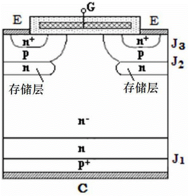
[0037] refer to figure 1 , the conductive channel of the existing CS-IGBT structure is on the surface, and its length is determined by the p base region and n + The difference in lateral junction depth of the emitter diffusion is determined. In addition, below the p base region there is a slightly higher concentration than the n - n-carrier storage layer in the drift region.

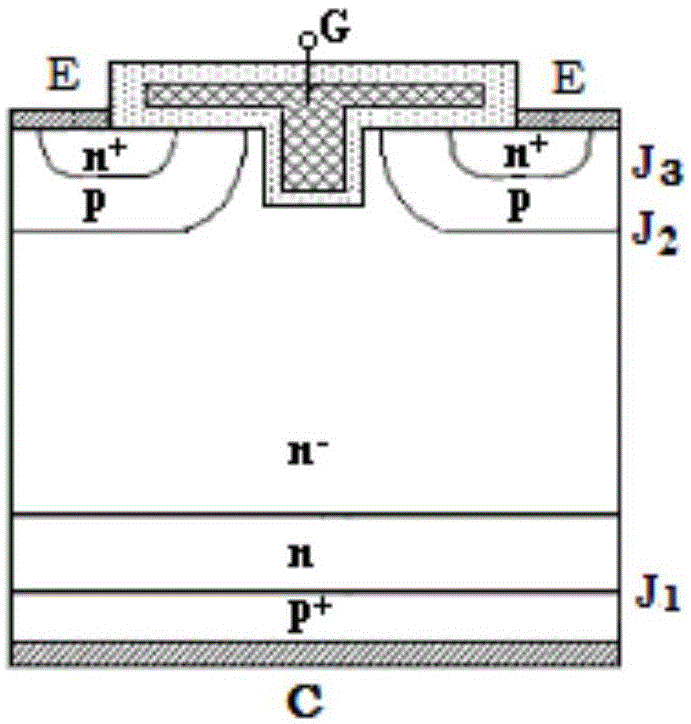
[0038] refer to figure 2 , the conductive channel of the existing TP-IGBT structure is also on the surface, only the n between the two p-base regions - A shallow groove is set above the drift region, and the depth of the groove is smaller than that of the p-base region, and the width of the groove is smaller than the distance between the p-base regions on both sides.

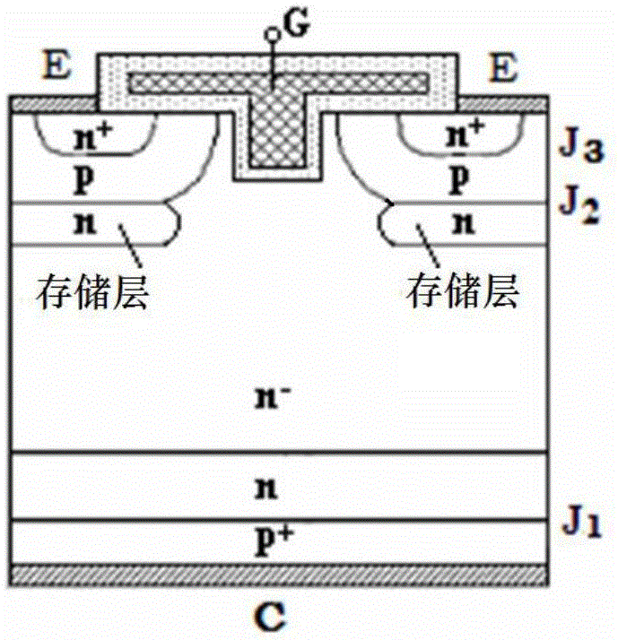
[0039] refer to image 3 , the electron injection enhanced high voltage IGBT structure of the p...


PUM

PropertyMeasurementUnit
Thicknessaaaaaaaaaa

Abstract

The invention discloses an electron injection enhanced high voltage IGBT. Gate oxide layers are arranged in a trench in a middle part on an n- silicon substrate and flat surface parts at two sides, and a polycrystalline silicon layer is arranged on the gate oxide layers, which is called a trench-planar gate G; two sides of the trench-planar gate G are each provided with a p base region on the n- silicon substrate, the p base regions are isolated from the trench-planar gate G through the gate oxides, and in each p base region an upper surface of an n+ emitter region and the p base region are short-circuited to form an emitting electrode E; joints of the upper side of an n- drift region and bottoms of the p base regions at the two sides are provided with discrete n carrier storage layers; and an n field stop layer, a p+ collector region and a collector electrode C are arranged in sequence under the n- drift region. The high voltage IGBT structure provided by the invention remarkably improves saturation voltage when a device is turned on, blocking voltage is high, on-state loss is low, and latch current density is relatively high.

Description

technical field [0001] The invention belongs to the technical field of power semiconductor devices, and relates to an electron injection-enhanced high-voltage IGBT, and also relates to a method for manufacturing the electron-injection enhanced high-voltage IGBT. Background technique [0002] One of the key technical issues that need to be solved in the development of high-voltage IGBTs is to reduce the saturation voltage in the on-state. In the existing planar gate IGBT and trench gate IGBT structures, a carrier storage (CS) layer is usually introduced to generate an electron injection enhancement effect, thereby increasing the conductance modulation during the turn-on period and reducing the saturation voltage. [0003] However, for the planar gate IGBT structure, although the CS layer can effectively reduce the saturation voltage and have a high short-circuit capability, it is still prone to latch-up at high temperatures, resulting in a decrease in the reliability of the d...

Claims


Application Information

Patent Timeline
IPC IPC(8): H01L29/739H01L21/331H01L29/06H01L29/423H01L21/28
CPCH01L21/28H01L29/06H01L29/423H01L29/66325H01L29/7393
Inventor 王彩琳井亚会
Owner XIAN SEMIPOWER ELECTRONICS TECH
Why Eureka
Try Eureka