Insulated-gate bipolar transistor with embedded island structure

A bipolar transistor, bipolar transistor technology, applied in semiconductor devices, electrical components, circuits, etc., can solve problems such as small improvement in forward saturation voltage drop, affecting device performance, and device forward withstand voltage drop. , to achieve the effect of reducing turn-off loss, improving carrier distribution, and reducing saturation voltage drop

Inactive Publication Date: 2012-12-26
UNIV OF ELECTRONICS SCI & TECH OF CHINA +1
View PDF6 Cites 16 Cited by
  • Summary
  • Abstract
  • Description
  • Claims
  • Application Information

AI Technical Summary

Problems solved by technology

However, the N-type carrier storage layer introduced by the above structure will increase the concentration of the N-type drift region under the P-type base region. If the concentration of the N-type carrier storage layer introduced is low, the hole barrier is small, The accumulation of holes is not obvious, and the improvement of forward...

Method used


Image

  • Insulated-gate bipolar transistor with embedded island structure
  • Insulated-gate bipolar transistor with embedded island structure
  • Insulated-gate bipolar transistor with embedded island structure

Examples


Embodiment Construction

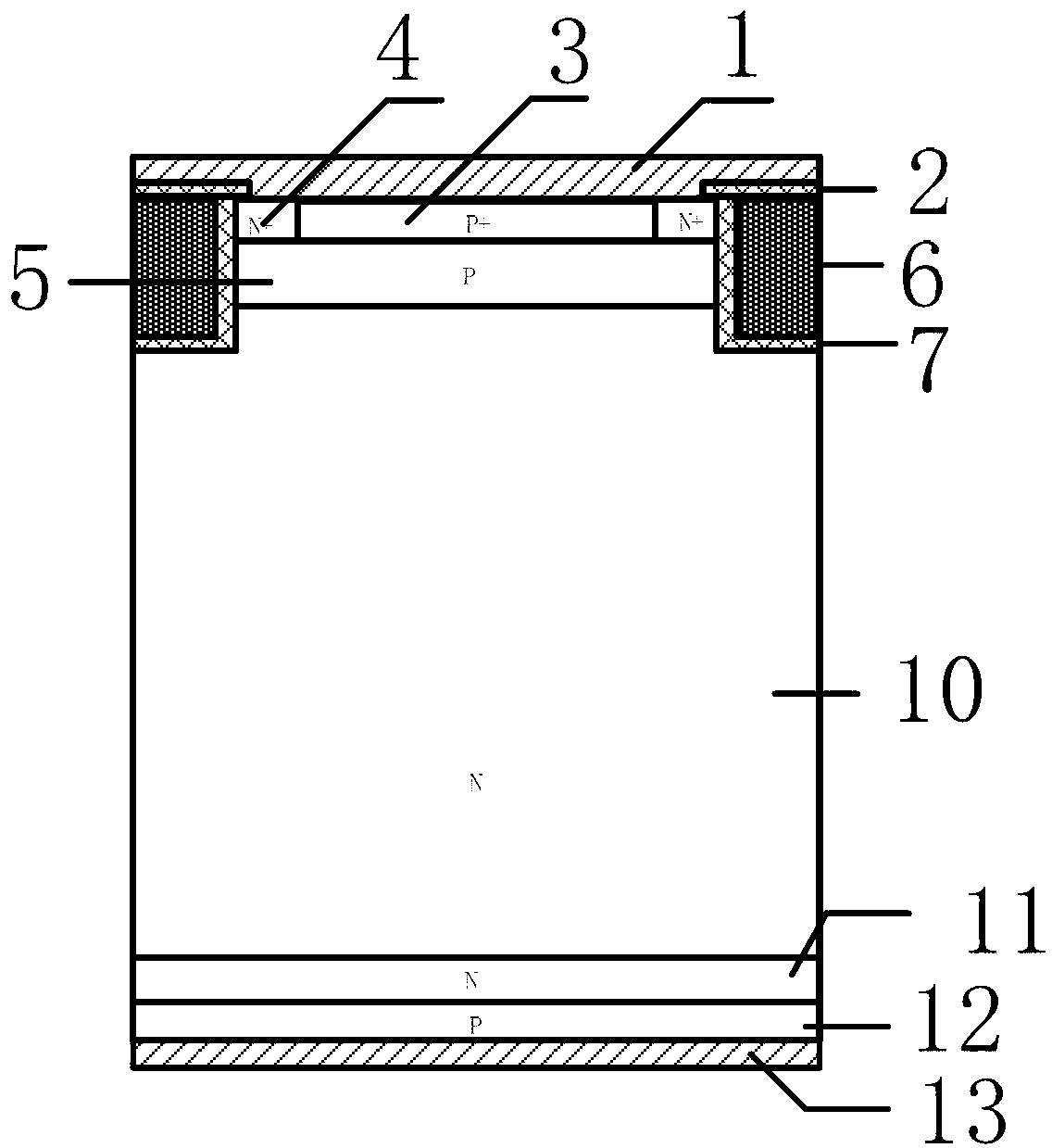
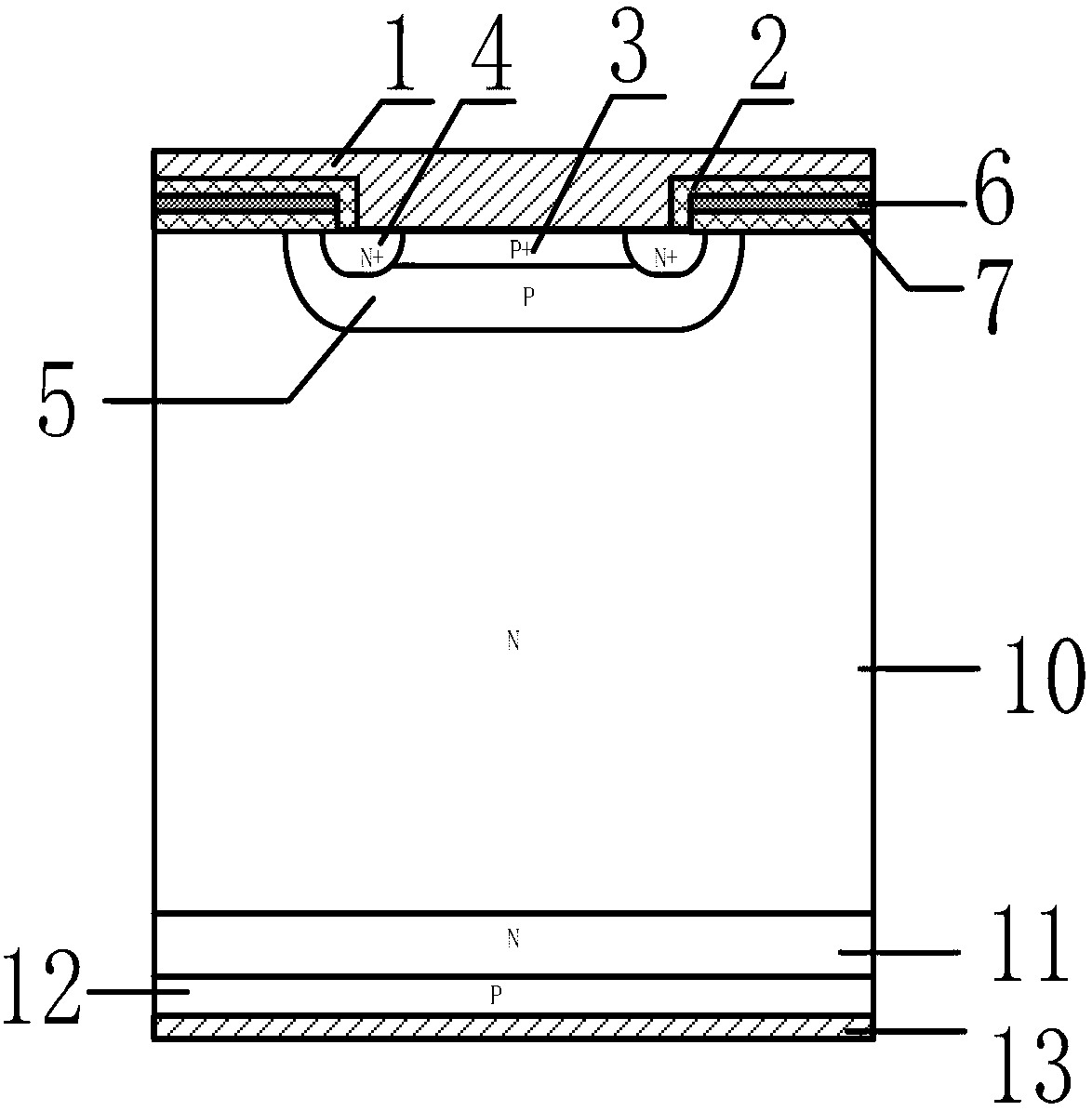
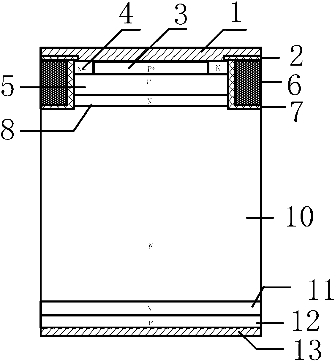
[0022] Insulated gate bipolar transistor with buried island structure, structure such as Figure 5 As shown, it includes a P+ collector region 12, a metal collector electrode 13 located on the back of the P+ collector region 12, an N+ electric field stop layer 11 located on the front of the P+ collector region 12, and an N-drift region 10 located on the N+ electric field stop layer 11. , the P-type base region 5 located in the middle of the top of the N-drift region 10, the two N+ source regions 4 located inside the P-type base region 5, the P+ source region located inside the P-type base region 5 and between the two N+ source regions 4 The contact region 3, the metal emitter 1 located on the device surface and in contact with the two N+ source regions 4 and the P+ contact region 3, the N-type charge storage layer 8 between the P-type base region 5 and the N-drift region 10; The two gate electrodes 6 on both sides of the device are connected to the N+ source region 4, the P-ty...


PUM


Abstract

An insulated-gate bipolar transistor with an embedded island structure belongs to the technical field of power semiconductor devices, and adopts a structure that a P-type embedded island and an N-type carrier storage layer structure are respectively introduced below the surface of an MOS (Metal Oxide Semiconductor) structure of a device. During forward blocking, the charge and the auxiliary electric field which are introduced by the P-type embedded island can weaken the peak electric field below the MOS structure so as to improve the voltage resistance of the device. During backward blocking, owing to high doping concentration or large thickness of the N-type carrier storage layer, the potential barrier of a cavity is lifted, the concentration of carriers near the emitting electrode is enhanced, accordingly, better carrier distribution is acquired, the forward saturation voltage drop of the device is reduced, better forward conduction voltage drop and turn-off loss compromise are obtained. The introduced P-type embedded island and N-type carrier storage layer are formed through ion implantation, epitaxy and other processes before the formation of a P-type base region. The insulated-gate bipolar transistor is suitable for the field of semiconductor power devices and power integrated circuits from low power to high power.

Description

technical field [0001] The invention belongs to the technical field of power semiconductor devices, and relates to an insulated gate bipolar transistor (IGBT). Background technique [0002] Power semiconductor technology is the core of power electronics technology. With the development of microelectronics technology, modern power semiconductor technology represented by gate-controlled power devices has developed rapidly since the 1980s, which has greatly promoted the progress of power electronics technology. . [0003] The power MOS tube is a voltage-controlled device, which can control the switching of the device by controlling the gate voltage. The structure of the driving circuit is simple, and the single-carrier conductivity makes it excellent in switching characteristics. However, multi-carrier conduction cannot produce conductance modulation effect in the drift region, so it is not suitable for medium and high voltage applications. At present, medium-high-voltage and...

Claims


Application Information

Patent Timeline
IPC IPC(8): H01L29/739H01L29/06
Inventor 张金平杨文韬李巍夏小军张灵霞李泽宏任敏张波
Owner UNIV OF ELECTRONICS SCI & TECH OF CHINA
Why Eureka
Try Eureka