Semiconductor device
a semiconductor device and semiconductor technology, applied in the direction of semiconductor devices, basic electric elements, electrical equipment, etc., can solve the problems of difficult to reduce the resistance of semiconductor devices, difficult to downsize the semiconductor device per unit cell, and non-negligeable resistan
- Summary
- Abstract
- Description
- Claims
- Application Information
AI Technical Summary
Benefits of technology
Problems solved by technology
Method used
Image

Examples
Embodiment Construction
[0030] The invention will be now described herein with reference to illustrative embodiments. Those skilled in the art will recognize that many alternative embodiments can be accomplished using the teachings of the present invention and that the invention is not limited to the embodiments illustrated for explanatory purposes.
[0031] The following paragraphs will describe one embodiment of a semiconductor device of the present invention, referring to the attached drawings.
[0032] It is to be noted that any common components in the drawings will be given with the same reference numerals, so as to dispense with repetitive explanation.
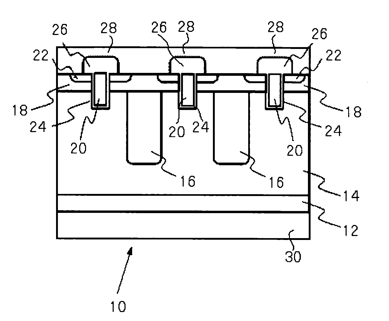
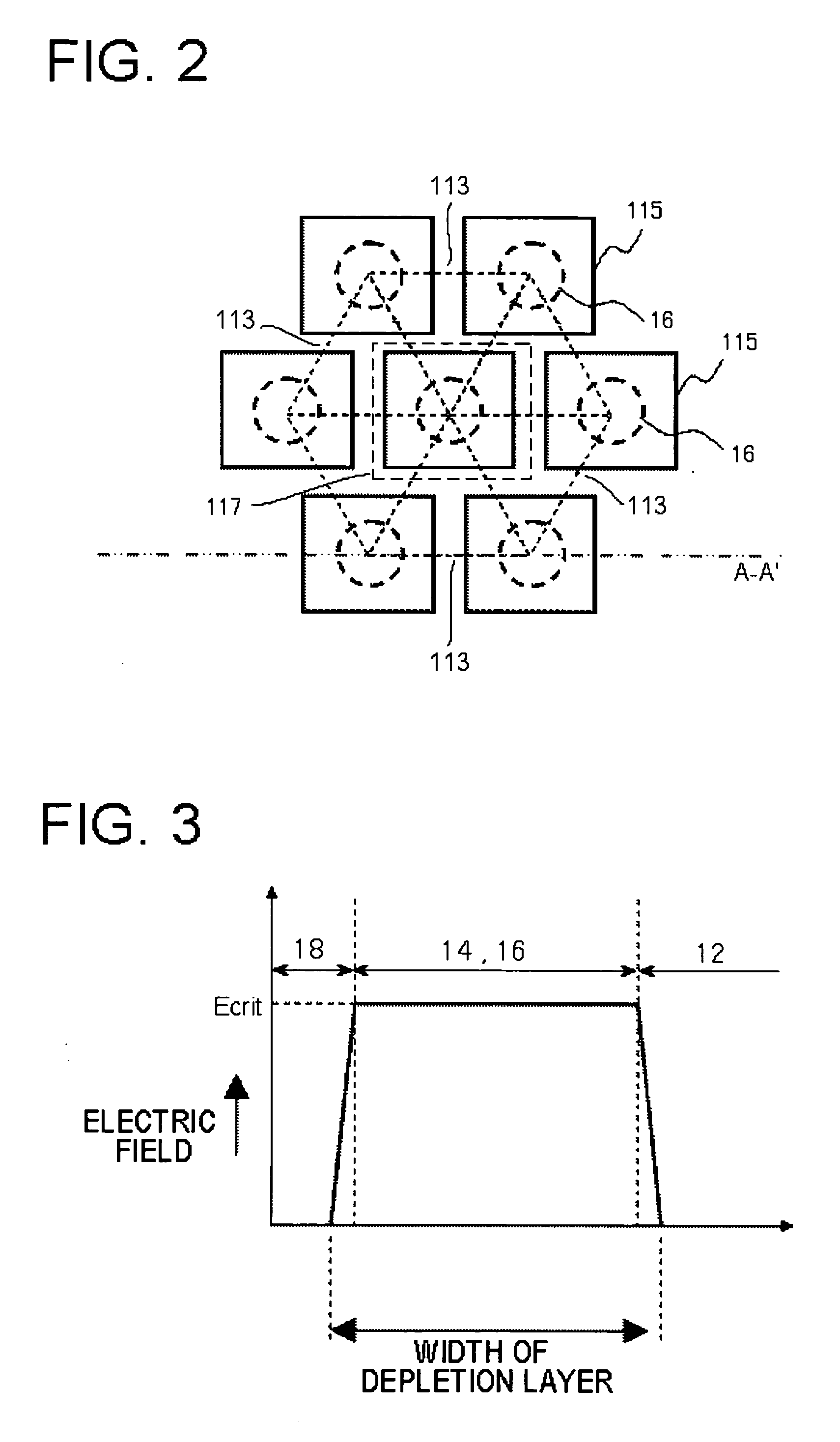
[0033]FIG. 1 is a sectional view of a semiconductor device of this embodiment, and FIG. 2 is a plan view of the semiconductor device shown in FIG. 1. FIG. 1 is a sectional view taken along line A-A′ in FIG. 2.
[0034] In this semiconductor device 10, an n+-type semiconductor substrate 12 which corresponds to the first-conductivity-type semiconductor substr...
PUM
 Abstract
Description
Claims
Application Information
 - R&D
- Intellectual Property
- Life Sciences
- Materials
- Tech Scout
- Unparalleled Data Quality
- Higher Quality Content
- 60% Fewer Hallucinations
Browse by: Latest US Patents, China's latest patents, Technical Efficacy Thesaurus, Application Domain, Technology Topic, Popular Technical Reports.
© 2025 PatSnap. All rights reserved.Legal|Privacy policy|Modern Slavery Act Transparency Statement|Sitemap|About US| Contact US: help@patsnap.com