Chip package structure, package substrate and manufacturing method thereof

a technology of chip packaging and substrate, which is applied in the direction of printed circuit aspects, basic electric elements, solid-state devices, etc., can solve the problems of limiting the bump pitch of a chip, increasing thermal stress and warpage between the two, and the packaging technology of the package substrate cannot keep up with the chip

Active Publication Date: 2006-04-13
ADVANCED SEMICON ENG INC
View PDF2 Cites 20 Cited by
  • Summary
  • Abstract
  • Description
  • Claims
  • Application Information

AI Technical Summary

Benefits of technology

[0007] Accordingly, one object of the present invention is to provide a package substrate capable of relaxing the space limit of pitches between bumps on a chip in the fabricating technology of package substrates.
[0008] Another object of the present invention is to provide a chip package structure having a flexible substrate specification.
[0009] Still another object of the present invention is to provide a method of fabricating a package substrate capable of relaxing the space limit of pitches between bumps on a chip in the fabricating technology of package substrates.
[0029] Accordingly, since the package substrate of the present invention utilizes an interposer for electrically connecting a first substrate and a chip together, the pitch of bumps on the chip is unaffected by the space limitation of the fabricating technology of the first substrate. Furthermore, because the package substrate connects with the chip through the interposer, and the interposer and the chip have similar thermal expansion coefficient, the flip chip device deploying the package substrate of the present invention have better bonding reliability. In addition, the interposer increases the heat-dissipating area of the chip. Hence, a flip chip device deploying the package substrate of the present invention can have a better thermal performance. Moreover, by modifying the circuit layout on the interposer, chips having different circuit layout can still use the package substrate of the present invention. Also, the chip location can be changed through a relocation of the interposer.

Problems solved by technology

However, the fabricating technology of the package substrate can hardly keep up with that of the chips.
Therefore, the current fabricating technology of the packaging substrate limits the bump pitch on a chip.
Furthermore, as the pad pitch continues to reduce, the mismatch of the coefficient of thermal expansion between the chip and the package substrate often leads to increasing thermal stress and warpage between the two.
Ultimately, the reliability of the connection between the chip and the package substrate declines.
In addition, the cost of fabricating a package substrate with fine pad pitch is very high.

Method used


Image

  • Chip package structure, package substrate and manufacturing method thereof
  • Chip package structure, package substrate and manufacturing method thereof
  • Chip package structure, package substrate and manufacturing method thereof

Examples


first embodiment

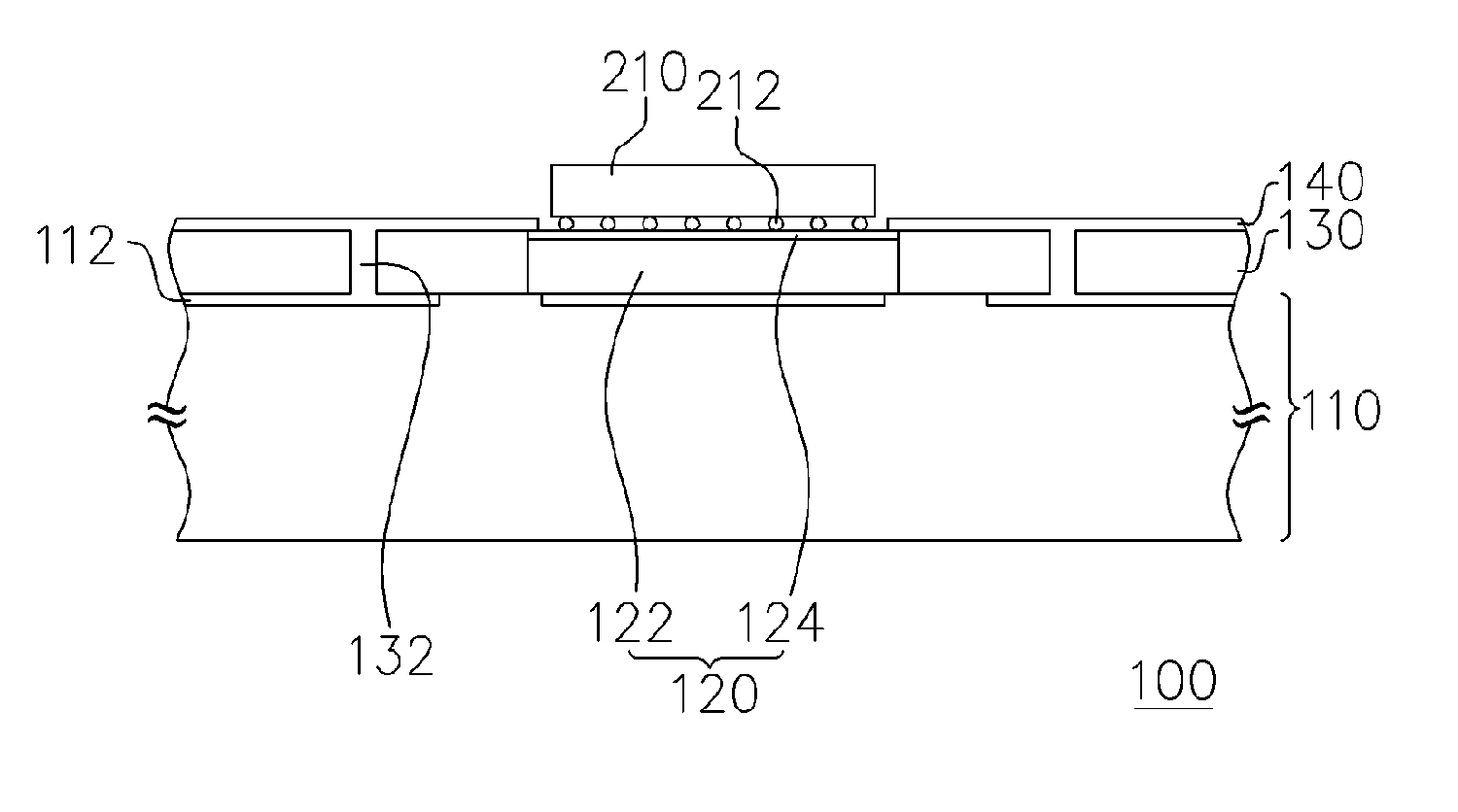
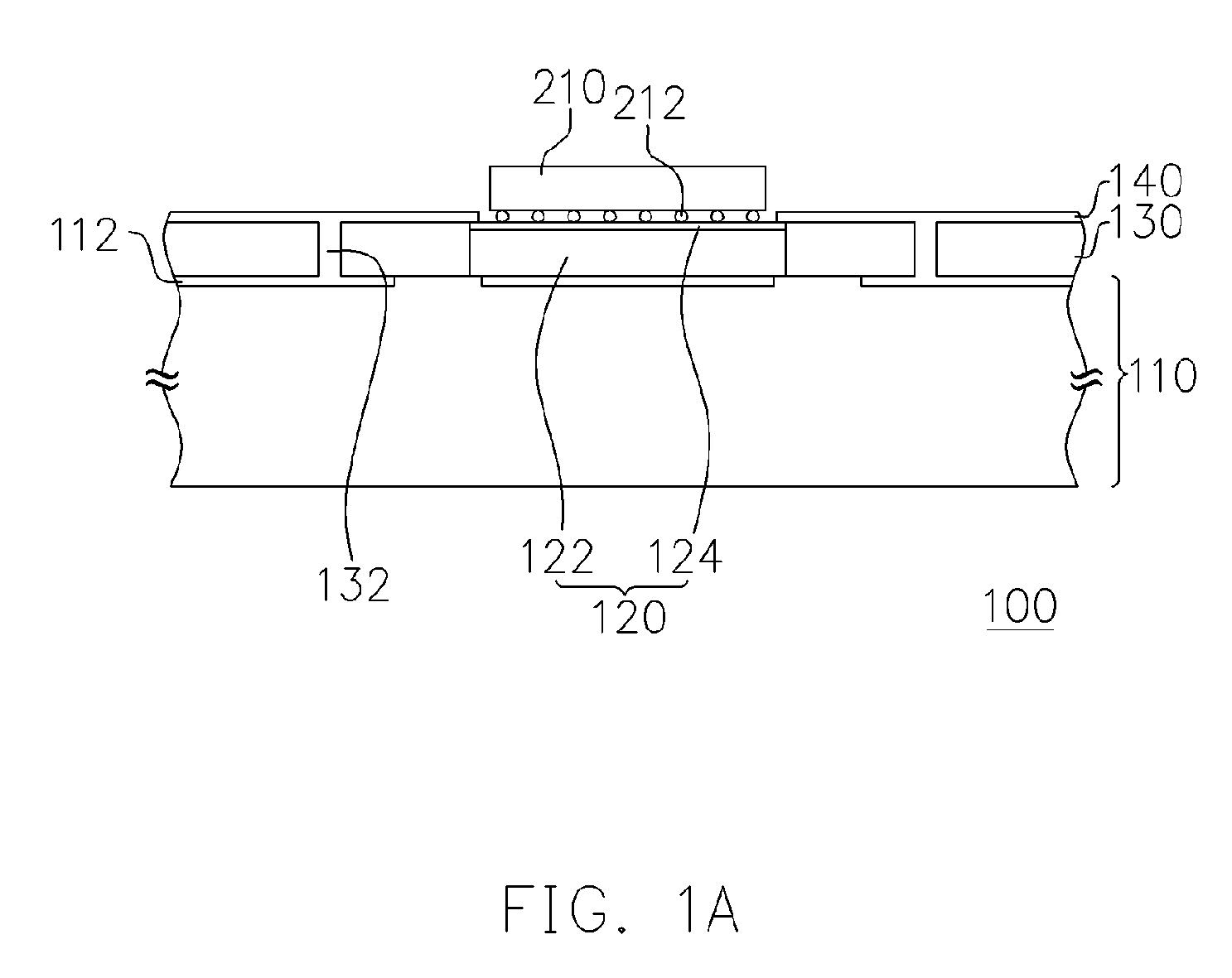
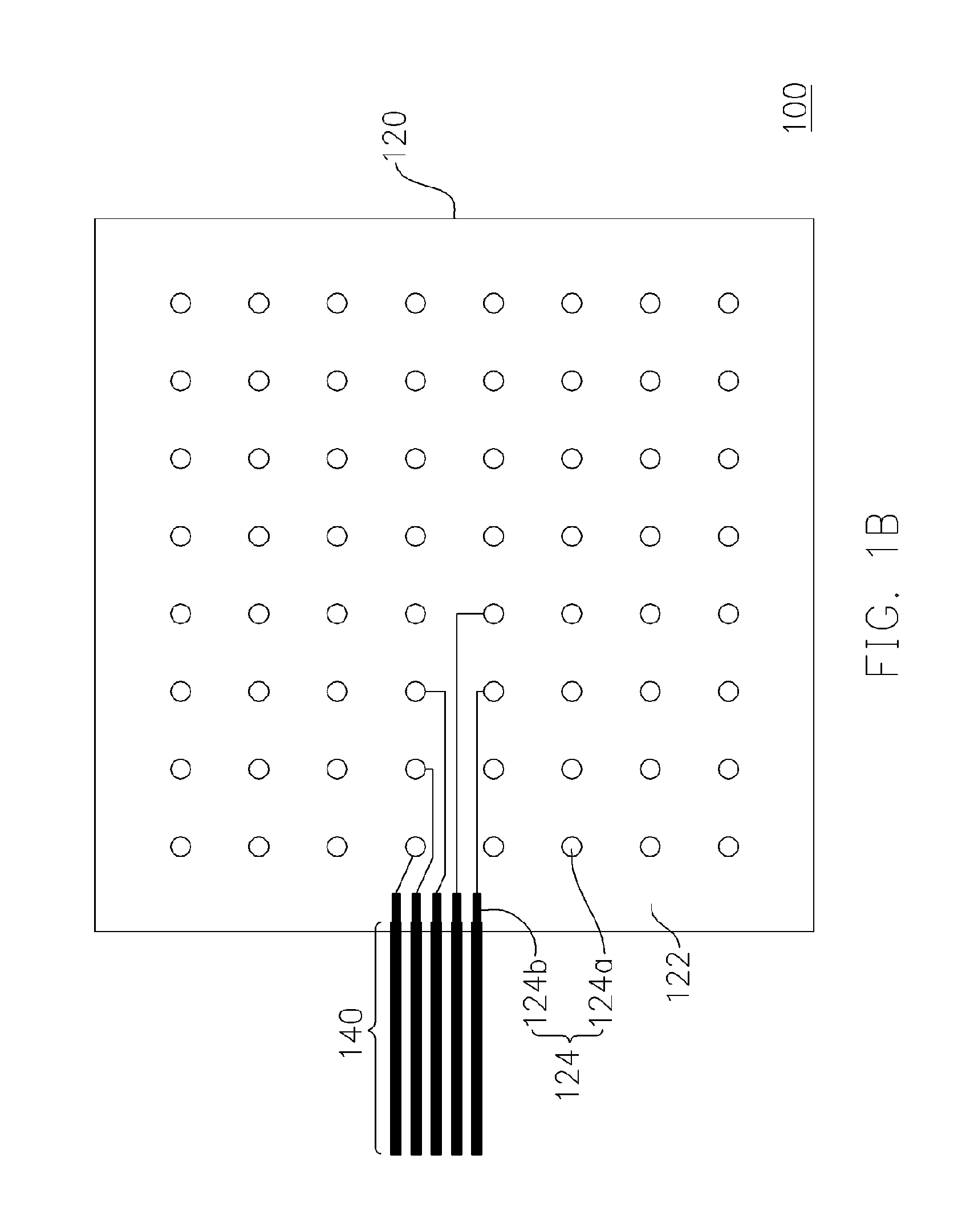
[0039]FIG. 1A is a schematic cross-sectional view showing the structure of a package substrate according to a first embodiment of the present invention. FIG. 1B is a top view of the package substrate according to the first embodiment of the present invention. As shown in FIGS. 1A and 1B, the package substrate 100 is designed to accommodate a chip 210 having a plurality of bumps 212 thereon. The package substrate 100 comprises a first substrate 110, an interposer 120, at least a dielectric layer 130 and at least a third circuit layer 140. The first substrate 110 has at least a first circuit layer 112 disposed on a surface thereof. In the present embodiment, the first substrate 110 doesn't be limited to a single-layer circuit board. The first substrate 110 may be a multi-layer circuit board.

[0040] The interposer 120 is disposed on the first substrate 110. The interposer 120 comprises a second substrate 122 and a second circuit layer 124. The second substrate 122 is disposed on the fi...

second embodiment

[0048]FIG. 3 is a schematic cross-sectional view showing the structure of a package structure according to a second embodiment of the present invention. In the second embodiment, the components same as those in the first embodiment are labeled with identical marks without further description.

[0049] The package substrate 100 as shown in FIG. 3 further comprises a solder mask layer 150 and an adhesion layer 160. The solder mask layer 150 covers the third circuit layer 140 and the dielectric layer 130 but exposes the interposer 120. The adhesion layer 160 is disposed between the interposer 120 and the first substrate 110. The interposer 120 is adhered to the first substrate 110 through an adhesion layer 160. Furthermore, the interposer 120 and the first substrate 110 can be connected together using other method beside the adhesion layer 160. In addition, there is no restriction on the method of electrically connecting the chip 210 to the interposer 120. Beside bumps 212, the chip 210 ...


PUM

PropertyMeasurementUnit
thicknessaaaaaaaaaa
thicknessaaaaaaaaaa
adhesionaaaaaaaaaa

Abstract

A package substrate for carrying a chip with a plurality of bumps thereon is provided. The package substrate includes a first substrate, and an interposer. The first substrate has a first circuit layer disposed on a surface thereof. The interposer includes a second substrate and a second circuit layer formed thereon. The second circuit layer comprises a plurality of bonding pads and traces. The traces are electrically connected to the corresponding bonding pads. Furthermore, the bonding pads are used for being connected to the bumps. The second circuit layer of the interposer is physically and electrically connected to the first circuit layer of the first substrate, and the second substrate and the first substrate are made of different materials.

Description

CROSS-REFERENCE TO RELATED APPLICATION [0001] This application claims the priority benefit of Taiwan application serial no. 93130958, filed on Oct. 13, 2004. All disclosure of the Taiwan application is incorporated herein by reference. BACKGROUND OF THE INVENTION [0002] 1. Field of the Invention [0003] The present invention relates to a substrate and manufacturing method thereof. More particularly, the present invention relates to a flip chip package substrate and manufacturing method thereof. [0004] 2. Description of the Related Art [0005] In the packaging process of integrated circuits (IC), the first level packaging mainly involves attaching chips onto carriers. The packaging formats include wire bonding (WB), tape automatic bonding (TAB) and flip chip (FC). Regardless of TAB or FC formats, in the process of attaching the chip onto the package substrate, bumps are fabricated on the bonding pads of a wafer so that the bumps can subsequently serve as an electrical connection betwee...

Claims


Application Information

Patent Timeline
Patent Type & Authority Applications(United States)
IPC IPC(8): H01L23/02H01L21/56H01L23/28
CPCH01L23/49833H01L2924/09701H05K1/142H05K1/183H05K2201/0187H05K2201/10378Y10T29/49155H01L2224/16Y10T29/4913Y10T29/49147Y10T29/49126Y10T29/49128H05K2201/10674
Inventor CHUNG, CHIH-MING
Owner ADVANCED SEMICON ENG INC
Why Eureka
Try Eureka