Method of manufacturing a casing of an electronic product with surface decoration thereon

a technology of electronic products and casings, which is applied in the direction of coatings, domestic applications, domestic articles, etc., can solve the problems of inability to provide precise quality, easy errors in the dimensions of decorative layers, and high cost of plates, so as to reduce manufacturing costs, facilitate surface decoration, and manufacture the effect of casings

Inactive Publication Date: 2006-04-13
PIN SHINE INDAL
View PDF8 Cites 7 Cited by
  • Summary
  • Abstract
  • Description
  • Claims
  • Application Information

AI Technical Summary

Benefits of technology

[0009] The primary object of the invention is therefore to specify a method of manufacturing a casing of an electronic product with surface decoration thereon, so that the design of surface decoration is easy and manufacturing of the casing is simple to reduce manufacturing costs thereof, and so that surface decoration is diverse and the quality thereof is improved to provide more types of exterior designs thereof for consumers.

Problems solved by technology

However, if the decorative layer is formed by coating, coloring and baking are alternately applied, which is time-consuming.
Also, errors in the dimensions of the decorative layer easily occur and the process cannot provide a precise quality.
If the decorative layer is formed by offset printing and serigraphy, the manufacturing efficiency is improved, but the costs of plates are expensive, making impossible to provide a market demand for both smaller quantity and diverse types to satisfy consumers' changes of their interests.
Also, the decorative layer has a grain surface, and the quality is not fine enough.
Furthermore, there are problems of adjustment and positioning when printing, which are complex and increase defective products.

Method used


Image

  • Method of manufacturing a casing of an electronic product with surface decoration thereon
  • Method of manufacturing a casing of an electronic product with surface decoration thereon
  • Method of manufacturing a casing of an electronic product with surface decoration thereon

Examples


Embodiment Construction

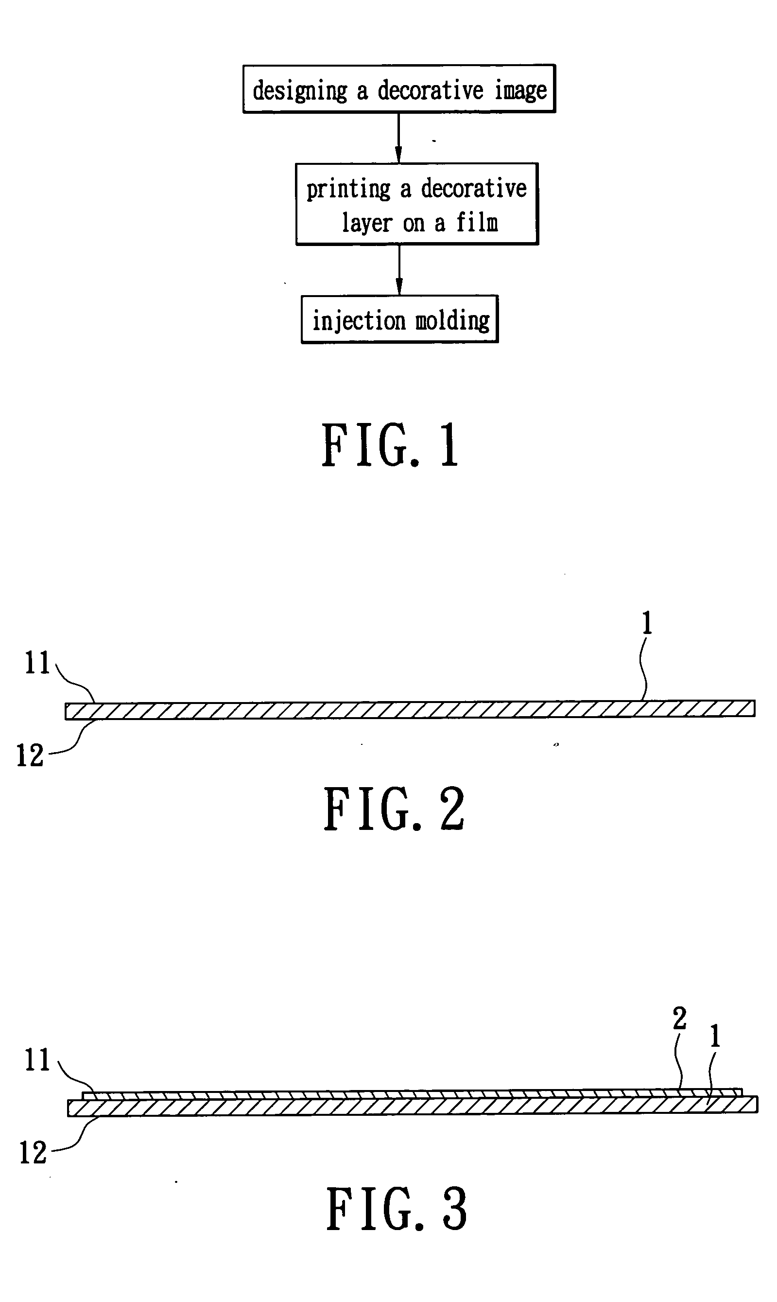
[0024]FIG. 1 illustrates a first embodiment of the present invention. The present invention provides a method of manufacturing a casing of an electronic product with surface decoration thereon. A decorative image is designed. Computerized image processing and printing equipment, such as a computer and a laser-type printer connected with each other, or a computer and an inkjet-type printer connected with each other, are provided. The computerized image processing and printing equipment are used to design a decorative image, such as, for example, drawings, written words, photos, trademarks, signatures, or graffiti.

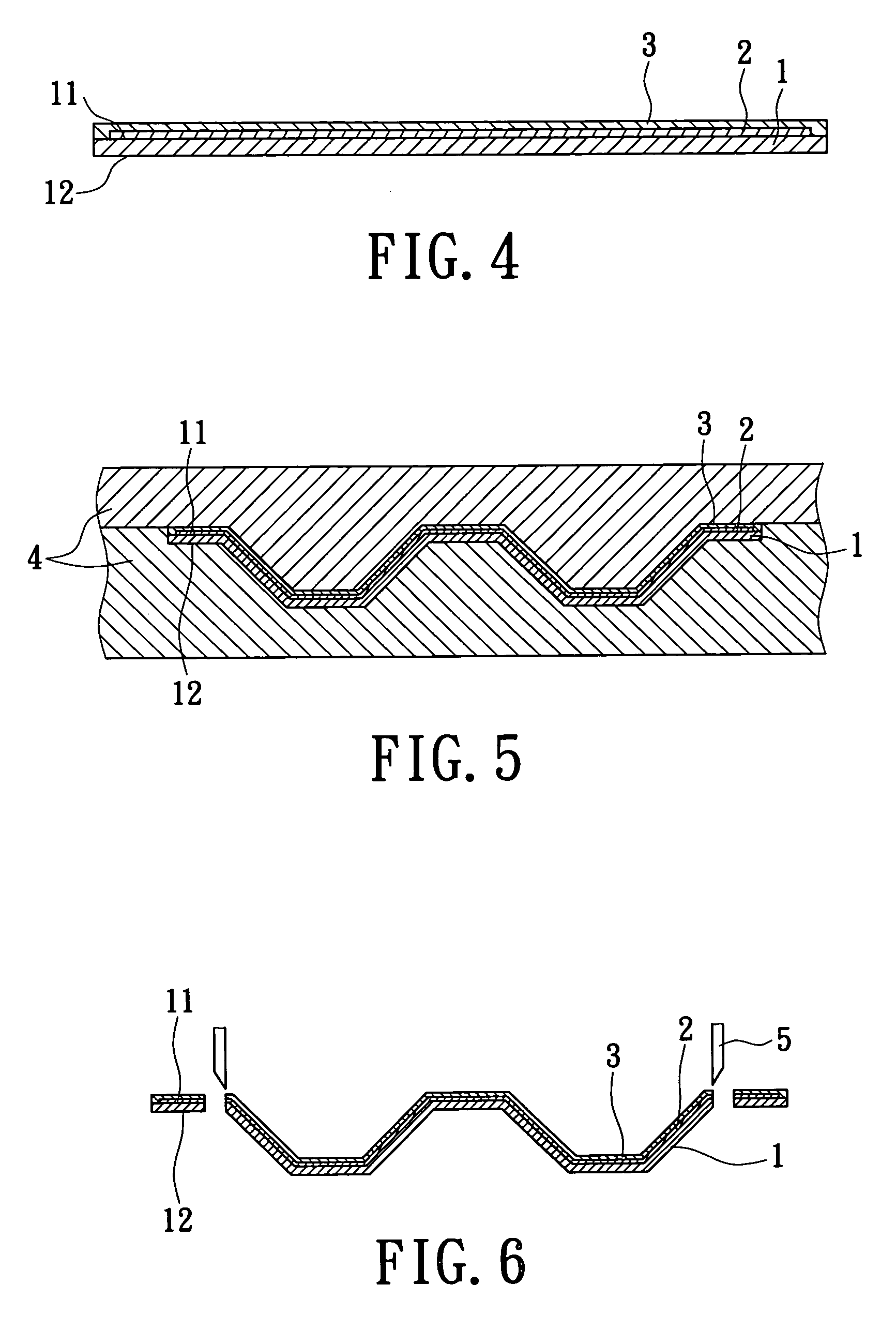
[0025] The decorative layer is then printed on a film. A film 1 (see FIG. 2) is provided, such as a plastic film made of PC material. The film 1 has a first surface 11 and a second surface 12. The computerized image processing and printing equipment are used to transform the decorative image into a decorative layer 2 and to print the decorative layer 2 on the film 1 (see FI...


PUM

PropertyMeasurementUnit
sizesaaaaaaaaaa
dimensionsaaaaaaaaaa
grain surfaceaaaaaaaaaa

Abstract

A method of manufacturing a casing of an electronic product with surface decoration thereon has a step of designing a decorative image, a step of printing a decorative layer on a film, and a step of injection molding. The decorative image is designed by using a computer. The decorative image is transformed into a decorative layer and the decorative layer is printed on a film by using a computer and a printer connected with each other. The casing of an electronic product with surface decoration thereof is obtained by applying in-mold decoration and injection molding technology, which combines injection material with the film.

Description

BACKGROUND OF THE INVENTION [0001] 1. Field of the Invention [0002] The present invention relates to a method of manufacturing a casing of an electronic product with surface decoration thereon, and more particularly, to a method of manufacturing a casing of an electronic product with surface decoration thereon that applies in-mold decoration and injection molding technology. [0003] 2. Background of the Invention [0004] Electronic products are used widely and have become an indispensable part of our lives. For example, portable electronic products, such as modern cellular phones, notebooks, hand-writing-type computers, personal digital assistants, multi-function portable drivers, or electronic learning dictionaries, have small sizes and many functions, and have become essential and practical tools in our lives and work. All such devices have decorative effects and fancy signs. Moreover, because imaginative designs are popular and the sense of individualized interests is raised, the k...

Claims


Application Information

Patent Timeline
Patent Type & Authority Applications(United States)
IPC IPC(8): B29C45/14B29C43/18
CPCB29C43/203B29C45/14688B29C2045/14737B29L2031/445
Inventor TSAI, FU-CHILIN, PO-YI
Owner PIN SHINE INDAL
Why Eureka
Try Eureka