
Solid immersion lens lithography

a technology of solid immersion lens and lithography, which is applied in the field of solid immersion lens lithography, can solve the problems of physical limits to the improvement of reduction lens

Active Publication Date: 2006-04-13
GLOBALFOUNDRIES US INC
View PDF18 Cites 8 Cited by
  • Summary
  • Abstract
  • Description
  • Claims
  • Application Information

AI Technical Summary

Benefits of technology

[0014] In accordance with another aspect of the present invention, a mask is provided that includes a plate capable of transmitting electromagnetic radiation. The plate includes at least one solid immersion lens. An opaque film is positioned on the plate. The opaque film is operable to allow transmission of the electromagnetic radiation through the at least one solid immersion lens but prevent transmission of the electromagnetic radiation through at least a portion of the plate.
[0015] In accordance with another aspect of the present invention, an apparatus is provided that includes a source of electromagnetic radiation and mask for passing selected portions of the electromagnetic radiation. The mask includes a plate capable of transmitting electromagnetic radiation. The plate includes at least one solid immersion lens and an opaque film on the plate. The opaque film is operable to allow transmission of the electromagnetic radiation through the at least one solid immersion lens but prevent transmission of the electromagnetic radiation through at least a portion of the plate.
[0016] In accordance with another aspect of the present invention, an apparatus is provided that includes a circuit device, a resist film positioned on the circuit device, a source of electromagnetic radiation, and a mask positioned between the source of electromagnetic radiation and the resist film for passing selected portions of the electromagnetic radiation to the resist film. The mask includes a plate capable of transmitting electromagnetic radiation. The plate includes at least one solid immersion lens and an opaque film on the plate. The opaque film is operable to allow transmission of the electromagnetic radiation through the at least one solid immersion lens but prevent transmission of the electromagnetic radiation through at least a portion of the plate.
[0017] In accordance with another aspect of the present invention, a method of manufacturing is provided that includes forming a resist film and exposing the resist film with radiation transmitted through a mask including a plate capable of transmitting electromagnetic radiation. The plate includes at least one solid immersion lens and an opaque film on the plate. Te opaque film is operable to allow transmission of the electromagnetic radiation through the at least one solid immersion lens but prevent transmission of the electromagnetic radiation through at least a portion of the plate.
[0018] A method of manufacturing is provided that includes forming at least one solid immersion lense on a plate capable of transmitting electromagnetic radiation, and forming an opaque film on the plate. The opaque film is operable to allow transmission of the electromagnetic radiation through the at least one solid immersion lens but prevent transmission of the electromagnetic radiation through at least a portion of the plate.

Problems solved by technology

However, there are still physical limits to the improvement of reduction lenses.

Method used


Image

  • Solid immersion lens lithography
  • Solid immersion lens lithography
  • Solid immersion lens lithography

Examples


Embodiment Construction

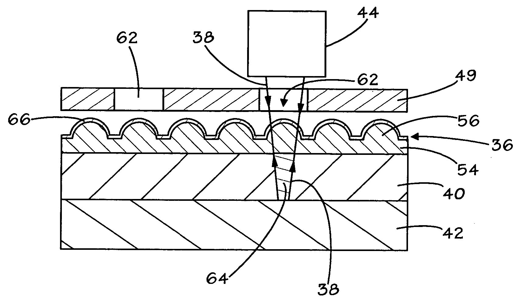
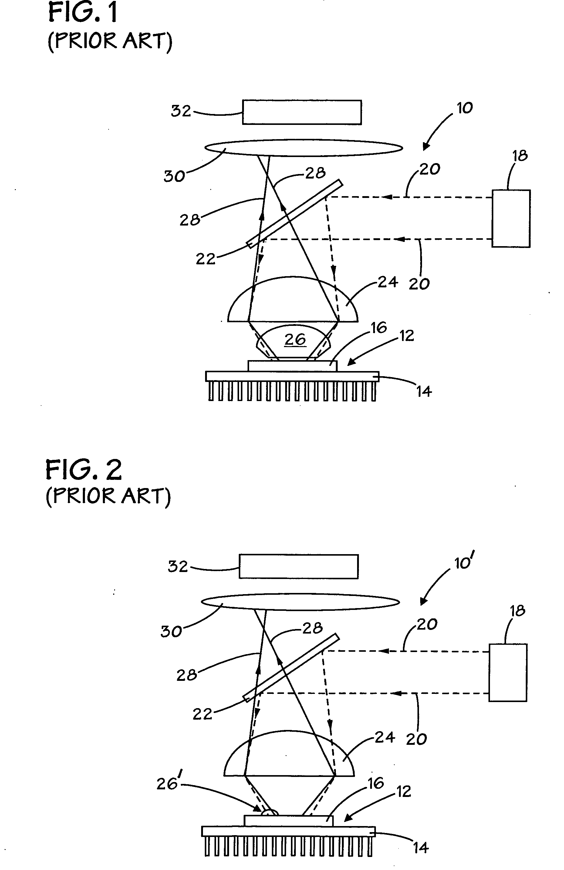
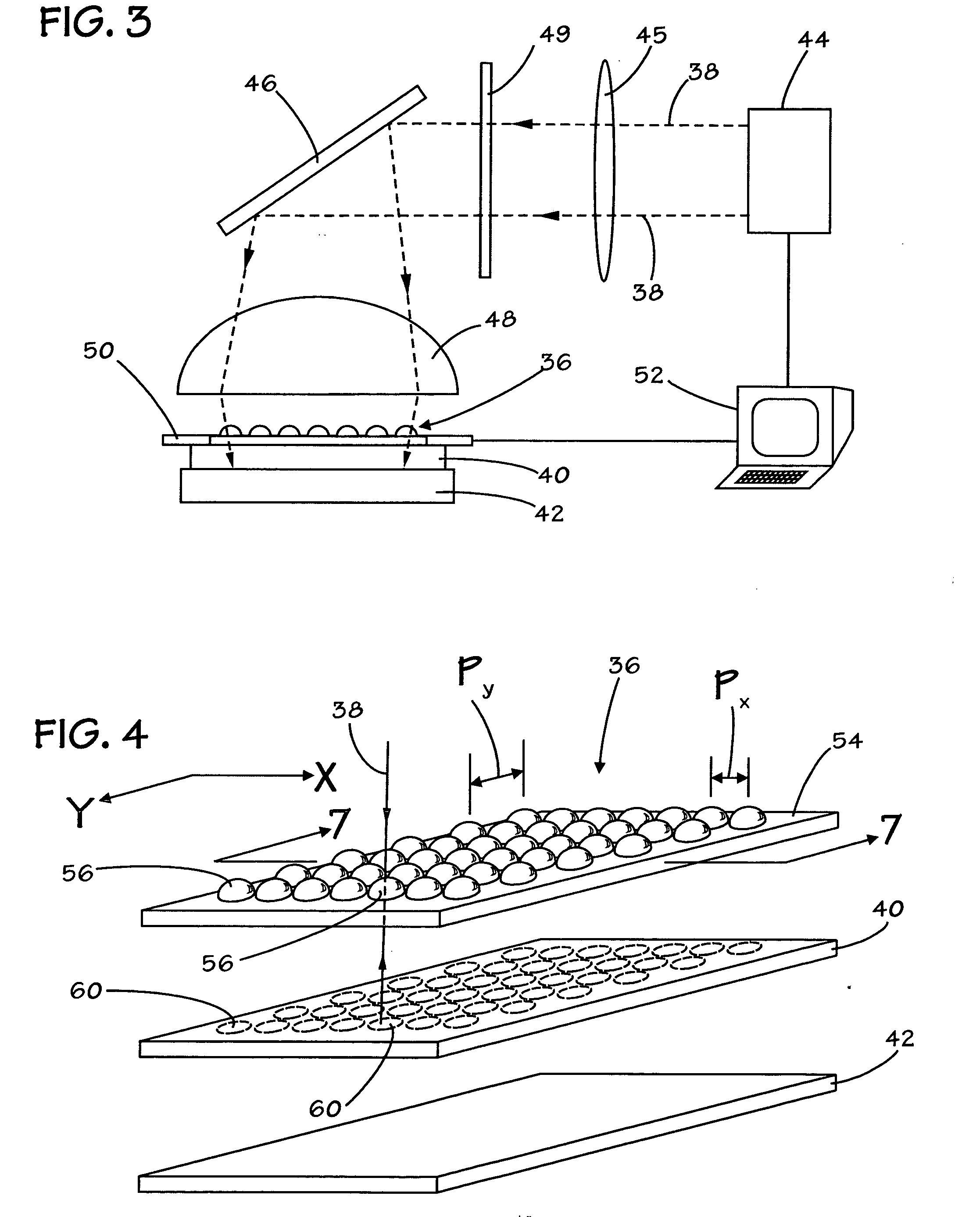
[0039] In the drawings described below, reference numerals are generally repeated where identical elements appear in more than one figure. Turning now to the drawings, and in particular to FIG. 1, therein is shown a side schematic view of an exemplary conventional solid immersion lens (“SIL”) microscope 10 that is used to image an integrated circuit 12. The integrated circuit 12 consists of a package 14 and an integrated circuit chip 16. The microscope 10 includes an illumination source 18 operable to deliver incident radiation 20 to a reflecting mirror or beam splitter 22. The incident rays 20 pass through an objective lens 24 and an underlying solid immersion lens 26. The solid immersion lens 26 focuses the incoming radiation 20 at a particular location or field of view on the chip 16. Reflected radiation 28 transmits back up through the solid immersion lens 26, the objective lens 24 and the beam splitter 22 where it is delivered to either an eye piece 30 or a camera 32 or both. I...


PUM

PropertyMeasurementUnit
Structureaaaaaaaaaa
Transmissionaaaaaaaaaa
Opacityaaaaaaaaaa

Abstract

Lithography using solid immersion lenses is disclosed. In one aspect, an apparatus is provided that includes a resist film that has a first side and a second and opposite side. One or more solid immersion lenses are positioned over the first side of the resist film. In another aspect, a method of manufacturing is provided that includes forming a resist film and exposing the resist film with radiation transmitted through one or more solid immersion lenses.

Description

BACKGROUND OF THE INVENTION [0001] 1. Field of the Invention [0002] This invention relates generally to semiconductor processing, and more particularly to methods and apparatus for lithographic patterning of structures. [0003] 2. Description of the Related Art [0004] The fabrication of modern integrated circuits requires the patterning of millions of different types of regions on a semiconductor wafer, such as local interconnect trenches, global metallization layers, and transistor gates, to name just a few. The manufacture of such multitudes of tiny structures is made possible by the use of lithographic processing. In photolithographic processing, a layer of photoresist material is applied to the wafer, frequently by spin-coating. Next, the photoresist layer is exposed to an actinic radiation source, such as deep ultraviolet (“DUV”). The DUV radiation is first passed through a mask or reticle that selectively transmits some of the DUV radiation while blocking other portions so that...

Claims


Application Information

Patent Timeline
IPC IPC(8): B29C47/96B29C47/92B29B13/00B29C35/12B28B17/00B29C35/08B29C47/00B29B15/00G03B27/42G03F1/00B29C48/92B29C48/96
CPCB82Y10/00B29C47/92G03F7/70325G03F7/20
Inventor GORUGANTHU, RAMA R.BRUCE, MICHAEL R.
Owner GLOBALFOUNDRIES US INC
Learn More