Self-emission display device and method of manufacturing the same

a display device and self-emission technology, applied in the direction of discharge tube luminescent screens, discharge tube/lamp details, electric discharge lamps, etc., can solve the problems of complex manufacturing process, inability to obtain the desired chromaticity, and white color displaying portions will be colored, so as to achieve uniform different brightness deteriorations of different luminescent colors

Inactive Publication Date: 2006-04-20
TOHOKU PIONEER CORP
View PDF9 Cites 0 Cited by
  • Summary
  • Abstract
  • Description
  • Claims
  • Application Information

AI Technical Summary

Benefits of technology

[0010] According to one aspect of the present invention, there is provided a self-emission display device in which self-emission elements of different luminescent colors are arranged in parallel or in a laminated manner, thereby enabling a color displaying by mixing a plurality of colors. In particular, self-emission elements of at least one of the plurality of luminescent colors have a luminescent functional layer whose electric current brightness efficiency degradation rate with respect to a driving time has been subjected to a lowering adjustment so as to make uniform different brightness deteriorations of different luminescent colors.
[0011] According to another aspect of the present invention, there is provided a method of manufacturing a self-emission display device in which self-emission elements of different luminescent colors are arranged in parallel or in a laminated manner, thereby enabling a color displaying by mixing a plurality of colors. Specifically, when forming a luminescent functional layer of self-emission elements of at least one of the plurality of luminescent colors, an electric current brightness efficiency degradation rate with respect to a driving time is subjected to a lowering adjustment so as to make uniform different brightness deteriorations of different luminescent colors.

Problems solved by technology

However, with regard to the aforementioned self-emission display device capable of color displaying, since the working life and the brightness deterioration extent of self-emission elements are different from one another due to different characteristics of different luminescent materials, a displaying performed during a long period can cause a color tone deviation, resulting in a problem that it is impossible to obtain a desired chromaticity.
Particularly, in displaying a white color in a base displaying portion or the like of a screen, there is a problem that the white color displaying portion will be colored during a long-period use.
However, with regard to the conventional technique disclosed in Japanese Unexamined Patent Application Publication No. 2001-290441, since different display devices of different product types require different panel designs, it is necessary each time to perform a patterning of apertures defining luminescent areas of luminescent zones, resulting in a complicated manufacturing process and making mass production difficult.
Moreover, since the foregoing apertures are formed by virtue of an insulating film pattern (which is for use before a film formation step), it becomes difficult for a substrate (for use before the film formation step) to ensure its universal use.
In addition, with regard to the conventional technique disclosed in Japanese Unexamined Patent Application Publication No. 2003-195817, it is necessary to include a specific circuit or the like to form a brightness adjusting unit, hence increasing the manufacturing cost.

Method used


Image

  • Self-emission display device and method of manufacturing the same
  • Self-emission display device and method of manufacturing the same
  • Self-emission display device and method of manufacturing the same

Examples


examples

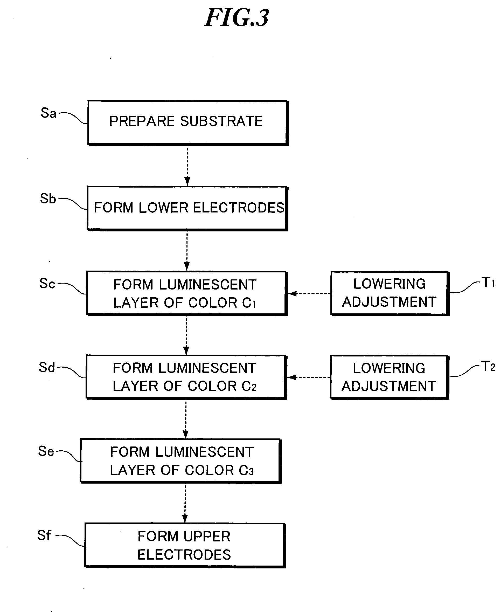
[0027] Next, description will be given to explain some examples of the present invention using organic EL elements as self-emission elements. However, the present invention should not be limited by these examples.

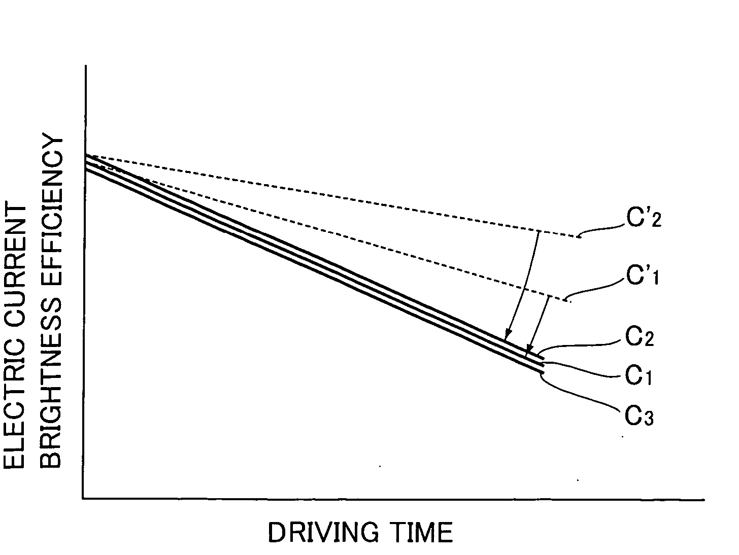
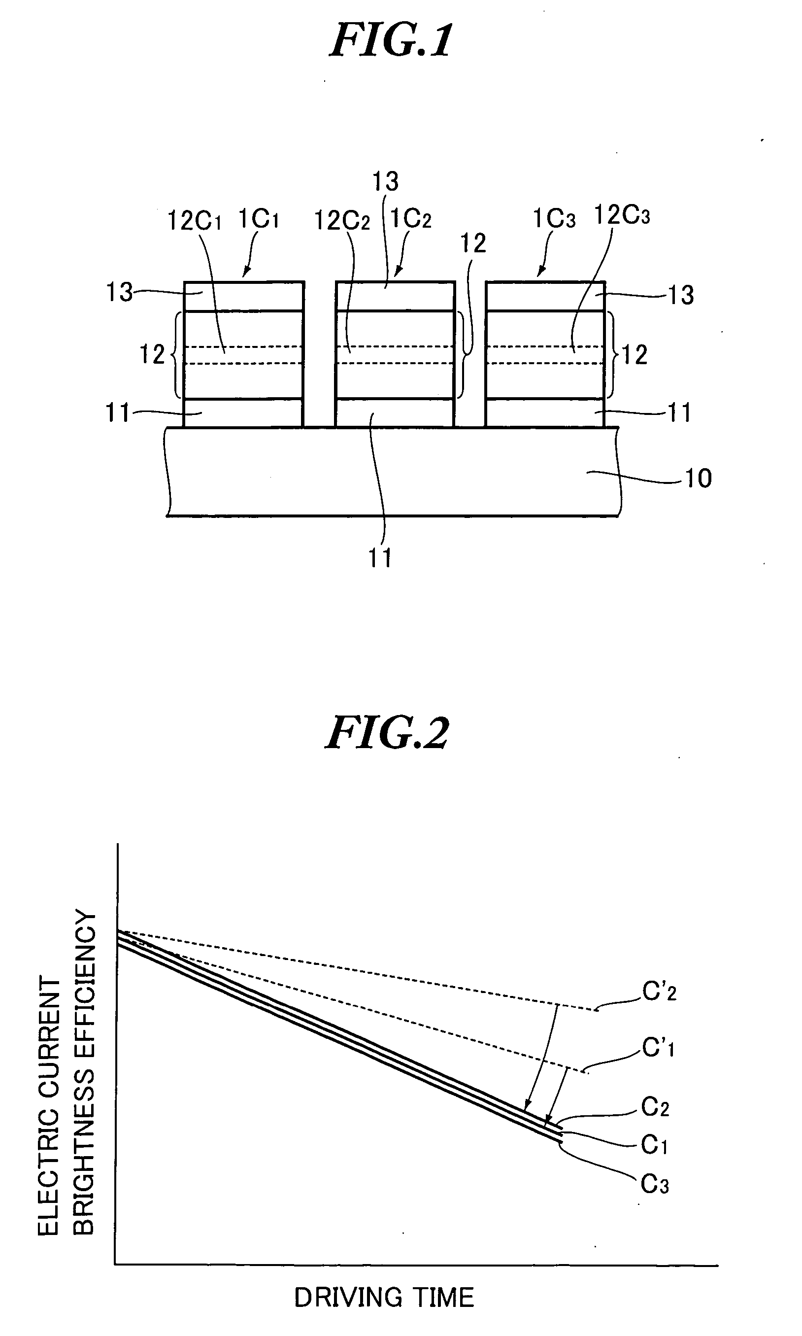
[0028] The following examples are given as compared to a comparative example which is directed to organic EL elements having luminescent layers of R (red), G (green) and B (blue) colors, while the light emission brightness efficiency of each color is set at its maximum value. In detail, Example 1 shows that lowering adjustment has been carried out by adjusting the concentration of luminescent material (dopant) added in luminescent layer. Example 2 shows that lowering adjustment has been carried out by adjusting the thickness of luminescent layer in addition to concentration adjustment.

example 1

[0035] Using the same materials and the same manufacturing process as the Comparative Example and setting the thicknesses of various layers of the laminated structures 12 at the same values as the Comparative Example, organic EL elements are formed by changing the dopant concentrations of R-luminescent layers and G-luminescent layers in a manner as shown in Table 2. In fact, Table 2 shows half value period lives when various luminescent elements of colors R, G, B have been driven by a constant electric current under a constant driving condition.

TABLE 2Example 1THICK-CONCEN-HALF VALUECOMPARATIVENESSTRATIONPERIOD LIFEEXAMPLE / COLOR[nm][%][h]EXAMPLER400.133500.333500.64900COMPARATIVEEXAMPLE1.533503.01550EXAMPLE6.0650G400.22790COMPARATIVEEXAMPLE0.71490EXAMPLE1.511003.0490B3.05.01610COMPARATIVEEXAMPLE / EXAMPLE

[0036] As clearly shown in Table 2, as compared to the Comparative Example, if the half value period life of R-luminescent layer is lower-adjusted from 4900 h to 1550 h by changing ...

example 2

[0038] The same materials and the same manufacturing process as the Comparative Example are used to change the dopant concentration and the thickness of each of R-luminescent layer and G-luminescent layer. Here, the dopant concentration of R-luminescent layer is adjusted to 0.3% and the dopant concentration of G-luminescent layer is adjusted to 0.7%, while the thickness of each of R-luminescent layer and G-luminescent layer is changed within a range of 10-40 nm. Table 3 shows half value period lives of various luminescent elements of colors R, G, B when they are driven by a constant electric current under a constant driving condition.

TABLE 3Example 2THICK-CONCEN-HALF VALUECOMPARATIVENESSTRATIONPERIOD LIFEEXAMPLE / COLOR[nm][%][h]EXAMPLER100.31480EXAMPLE252620403350400.64900COMPARATIVEEXAMPLEG100.7956251326401490EXAMPLE400.22790COMPARATIVEEXAMPLEB305.01610COMPARATIVEEXAMPLE / EXAMPLE

[0039] As clearly shown in Table 3, with respect to the Comparative Example, if the half value period li...


PUM


Abstract

It is an object of the present invention to prevent a color tone deviation during a long-period use, so as to improve a displaying quality of a display device. Another object of the present invention is to ensure a universal use of each substrate and to prevent a complication of manufacturing process. The present invention is based on a self-emission display device in which self-emission elements of different luminescent colors are arranged in parallel or in a laminated manner, thereby enabling a color displaying by mixing a plurality of different colors. A luminescent layer of a self-emission element and a luminescent layer of another self-emission element are subjected to lowering adjustments of C1′→C1 and C2′→C2, so as to make uniform brightness deteriorations which are originally different due to different luminescent colors.

Description

BACKGROUND OF THE INVENTION [0001] The present invention relates to a self-emission display device and a method of manufacturing the same. [0002] The present application claims priority from Japanese Application No. 2004-300322, the disclosure of which is incorporated herein by reference. [0003] A self-emission display device having (as its essential elements) self-emission elements such as organic EL elements can perform a flat panel displaying and this realizes a reduced power consumption and an increased displaying brightness as compared to a liquid crystal display for which back light is indispensable. [0004] In performing a color (full color or multi-color) displaying using the aforementioned self-emission display device, it is usual to arrange self-emission elements of different luminescent colors in parallel or in a laminated manner in display units (pixels) so as to perform a color displaying by mixing a plurality of colors. Generally, in performing a full color displaying, ...

Claims


Application Information

Patent Timeline
Patent Type & Authority Applications(United States)
IPC IPC(8): H05B33/14H05B33/18
CPCH01L27/3211H01L51/5036H10K59/35H10K50/125H05B33/22H05B33/10
Inventor YUKI, TOSHINAONAKAMURA, MASATO
Owner TOHOKU PIONEER CORP
Why Eureka
Try Eureka