Plasma display panel (PDP) and its method of manufacture

a technology of plasma display panel and display panel, which is applied in the manufacture of electrodes, electrode systems, electric discharge tubes/lamps, etc., can solve the problem of overloaded driving circuit of pdp, and achieve the effect of reducing voltage margin variation and increasing overall voltage margin

Inactive Publication Date: 2006-04-20
SAMSUNG SDI CO LTD
View PDF16 Cites 2 Cited by
  • Summary
  • Abstract
  • Description
  • Claims
  • Application Information

AI Technical Summary

Benefits of technology

[0018] The present invention provides a PDP which reduces a variation among voltage margins of Red, Green, and Blue phosphor layers by differentiating thicknesses of dielectric layers that bury discharge electrodes corresponding to discharge cells coated with the R, G, and B phosphor layers, thereby increasing the overall voltage margin, and a method of manufacturing the PDP.

Problems solved by technology

Thus, a driving circuit for the PDP is overloaded.

Method used


Image

  • Plasma display panel (PDP) and its method of manufacture
  • Plasma display panel (PDP) and its method of manufacture
  • Plasma display panel (PDP) and its method of manufacture

Examples


Embodiment Construction

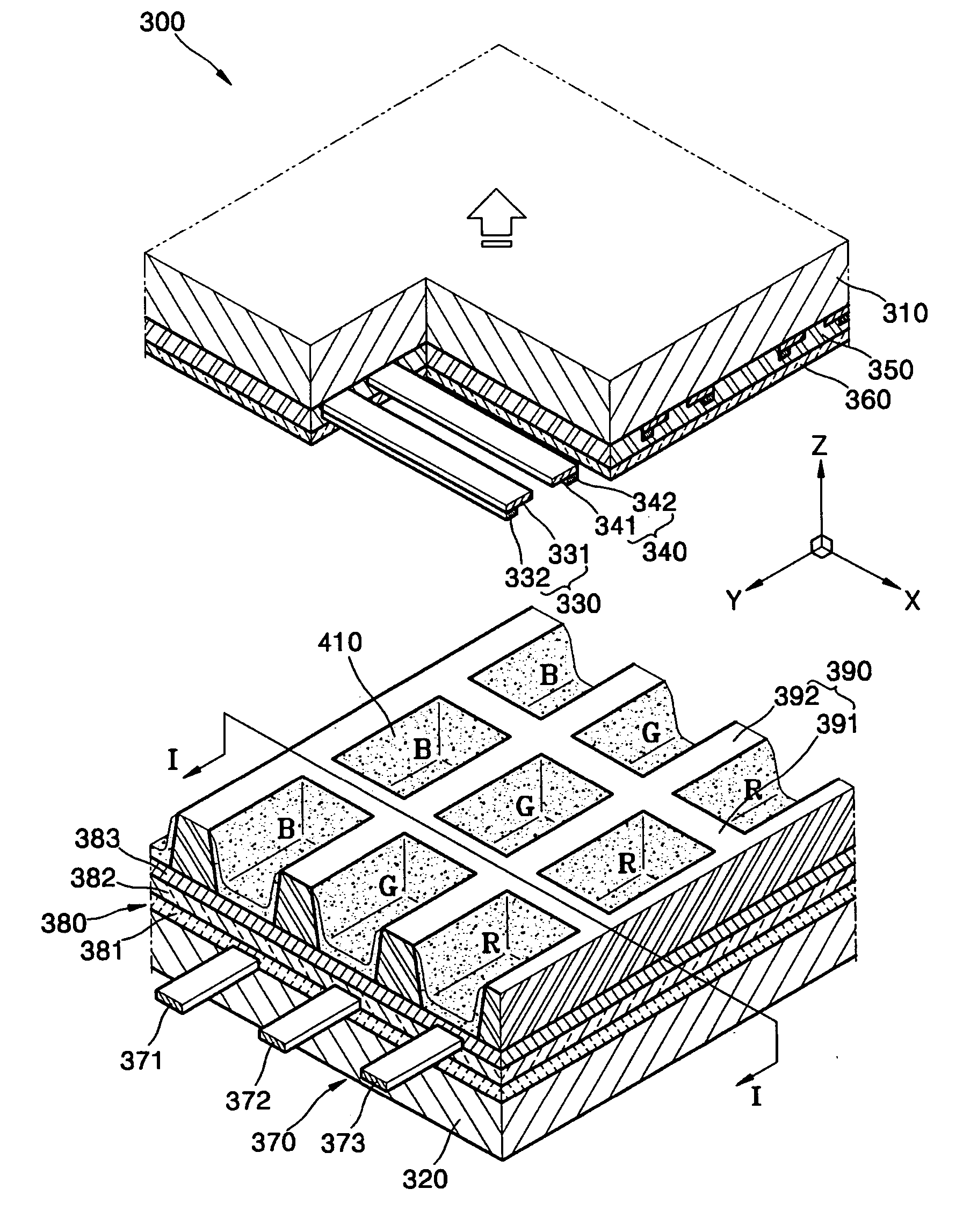
[0048]FIG. 1 is an exploded perspective view of a three-electrode surface discharge PDP 100. Referring to FIG. 1, the PDP 100 includes a front substrate 110 and a rear substrate 120, which are arranged to face each other.

[0049] X and Y electrodes 130 and 140 are arranged on an inner surface of the front substrate 110 in such a way that an X electrode 130 and a Y electrode 140 are both located within each discharge cell. The X electrode 130 includes a first electrode line 131, which is transparent, and a first bus electrode 132, which is overlapped by the first electrode line 131. The Y electrode 140 includes a second electrode line 141, which is transparent, and a second bus electrode 142, which is overlapped by the second electrode line 141. The X and Y electrodes 130 and 140 are buried in a front dielectric layer 150. The front dielectric layer 150 is coated with a protective layer 160.

[0050] Address electrodes 170 are arranged on an inner surface of the rear substrate 120 to cr...


PUM


Abstract

A Plasma Display Panel (PDP) and its method of manufacture includes: a first substrate; a plurality of first discharge electrodes arranged on the first substrate; a second substrate arranged opposite to the first substrate and in parallel therewith; a plurality of second discharge electrodes arranged on the second substrate to cross the first discharge electrodes, the second discharge electrodes being adapted to be addressed with the first discharge electrodes and located on different levels; barrier ribs disposed between the first and second substrates to define discharge cells; and Red (R), Green (G), and Blue (B) phosphor layers coated on lateral sides of the barrier ribs. Address electrodes for discharge cells coated with R, G, and B phosphor layers are positioned on different levels, so that address voltages become more uniform regardless of the color of a phosphor layer.

Description

CLAIM OF PRIORITY [0001] This application makes reference to, incorporates the same herein, and claims all benefits accruing under 35 U.S.C.§119 from an application for PLASMA DISPLAY PANEL AND METHOD OF MANUFACTURING THE SAME earlier filed in the Korean Intellectual Property Office on 19 Oct. 2004 and there duly assigned Serial No. 10-2004-0083499. BACKGROUND OF THE INVENTION [0002] 1. Field of the Invention [0003] The present invention relates to a Plasma Display Panel (PDP), and more particularly, to a PDP that can be driven with a low voltage by differentiating thicknesses of dielectric layers that bury discharge electrodes, and its method of manufacture. [0004] 2. Description of the Related Art [0005] Typically, Plasma Display Panels (PDPs) are flat display panels that display desired numbers, characters, or graphics by discharging a gas injected between two substrates each having discharge electrodes and exciting a phosphor layer using ultraviolet rays generated from the disch...

Claims


Application Information

Patent Timeline
Patent Type & Authority Applications(United States)
IPC IPC(8): H01J17/49H01J9/02H01J9/227H01J11/12H01J11/22H01J11/24H01J11/26H01J11/32H01J11/34H01J11/38H01J11/40H01J11/42H01J11/50
CPCH01J9/02H01J11/12H01J11/26H01J11/32H01J11/38H01J2211/326
Inventor SONG, JUNG-SUK
Owner SAMSUNG SDI CO LTD
Why Eureka
Try Eureka