Silicon carbide power semiconductor module device integrated with buffer circuit

A power semiconductor and snubber circuit technology, which is applied in the field of silicon carbide power semiconductor devices, can solve problems such as long turn-on time, voltage drop, and high turn-on loss, and achieve the goals of improving reliability and efficiency, reducing switching loss, and reducing conduction loss Effect

Pending Publication Date: 2021-10-26
GUANGHUA LINGANG ENG APPL & TECH R&D (SHANGHAI) CO LTD
View PDF4 Cites 0 Cited by
  • Summary
  • Abstract
  • Description
  • Claims
  • Application Information

AI Technical Summary

Problems solved by technology

However, the passive snubber circuit is packaged in the SiC power semiconductor module, which will cause a voltage drop when the SiC power semiconductor module is turned on, resulting in longer turn-on time and higher turn-on loss

Method used


Image

  • Silicon carbide power semiconductor module device integrated with buffer circuit
  • Silicon carbide power semiconductor module device integrated with buffer circuit
  • Silicon carbide power semiconductor module device integrated with buffer circuit

Examples


Embodiment Construction

[0019] In order to make the purposes, technical solutions and advantages of the embodiments of the present application clearer, the technical solutions in the embodiments of the present application will be clearly and completely described below in conjunction with the drawings in the embodiments of the present application. Obviously, the described embodiments It is a part of the embodiments of this application, not all of them. Based on the embodiments in this application, all other embodiments obtained by persons of ordinary skill in the art without creative efforts fall within the protection scope of this application.

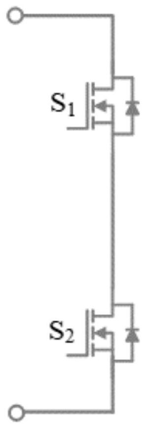
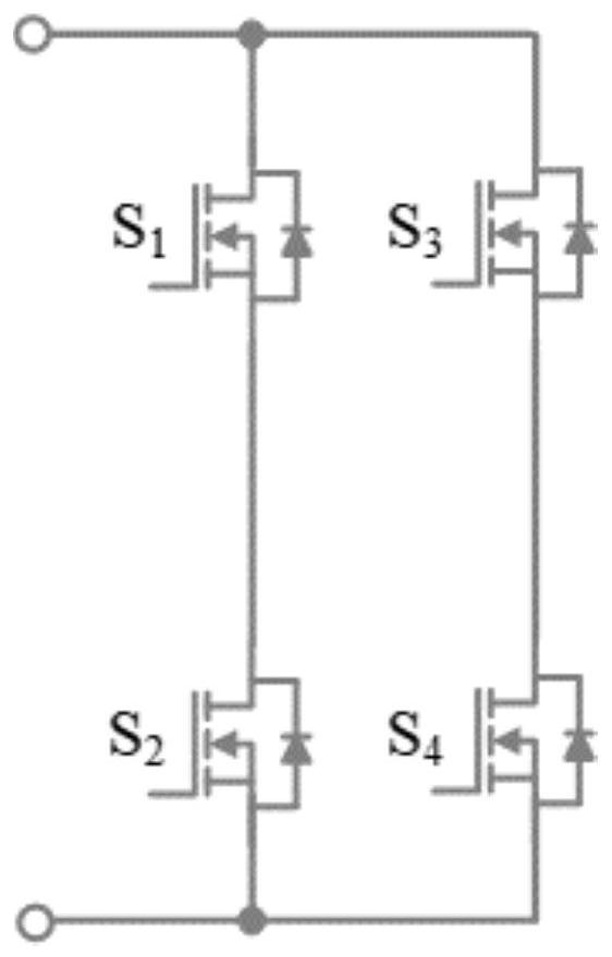
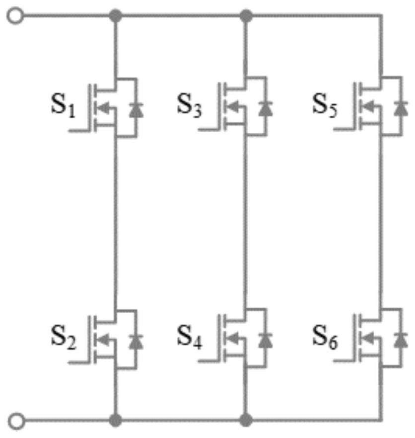
[0020] Figure 5 It is a schematic diagram of the circuit principle of the three-phase silicon carbide power semiconductor module device integrated with the active snubber circuit of the present invention. Package integrated active snubber circuits in single-phase half-bridge, single-phase full-bridge or three-phase bridge SiC power semiconductor modules, su...


PUM


Abstract

The invention provides a silicon carbide power semiconductor module device integrated with a buffer circuit. An active buffer circuit is integrated in a single-phase half-bridge, single-phase full-bridge or three-phase bridge type silicon carbide power semiconductor module, so that the switching loss of the silicon carbide power semiconductor module can be reduced, the oscillation and damping loss can be reduced, the voltage peak can be reduced, the silicon carbide power semiconductor module can work at a higher voltage, or a low-voltage-grade chip is selected to reduce the conduction loss, and the efficiency of the silicon carbide power electronic system is improved.

Description

technical field [0001] The present application relates to the technical field of silicon carbide power semiconductor devices, in particular to a silicon carbide power semiconductor module device with an integrated buffer circuit. Background technique [0002] Silicon carbide power semiconductor modules are widely used in half-bridge circuits, full-bridge circuits and three-phase bridge circuits ( Figure 1 ~ Figure 3 ), due to the serious electromagnetic interference and noise caused by high-speed switching of SiC MOSFETs, the parasitic inductance of SiC power semiconductor modules will bring high oscillation and voltage spikes. Integrating packaged passive snubber circuits in SiC power semiconductor modules such as Figure 4 As shown, the oscillation and voltage spikes of three-phase SiC power semiconductor modules can be reduced, thereby improving the efficiency and reliability of SiC power electronic systems. However, the passive snubber circuit is packaged in the silico...

Claims


Application Information

Patent Timeline
Patent Type & Authority Applications(China)
IPC IPC(8): H02M1/34H01L29/78
CPCH02M1/34H01L29/78Y02B70/10
Inventor 杨书豪王志坤
Owner GUANGHUA LINGANG ENG APPL & TECH R&D (SHANGHAI) CO LTD
Why Eureka
Try Eureka