Plasma display panel and method of manufacturing the same

a technology of display panel and substrate, which is applied in the manufacture of electrode systems, electrical discharge tubes/lamps, and electrodes, etc., can solve the problems of lack of uniformity, interference of light, and lack of uniform transmittance in the substrate on the front side, so as to achieve high uniformity and lack of uniformity in display.

Inactive Publication Date: 2006-04-20
FUJITSU HITACHI PLASMA DISPLAY LTD
View PDF13 Cites 7 Cited by
  • Summary
  • Abstract
  • Description
  • Claims
  • Application Information

AI Technical Summary

Benefits of technology

[0014] According to the present invention, the difference in the index of refraction between the dielectric layer and the protective film is not greater than 0.20 in the substrate on the front side, and therefore

Problems solved by technology

Concerning the optical properties of this substrate on the front side, it is known that interference of light occurs because the protective film is a thin film.
Such interference properties differ, depending on the film thickness, and therefore, there is lack of uniformity in the transmittance in the substrate on the front side, in the case where there is lack of uniformity in the film thickness of the protective film within the panel surface.
However, it is considered that a difference of 70 nm in the film thickne

Method used


Image

  • Plasma display panel and method of manufacturing the same
  • Plasma display panel and method of manufacturing the same
  • Plasma display panel and method of manufacturing the same

Examples


Embodiment Construction

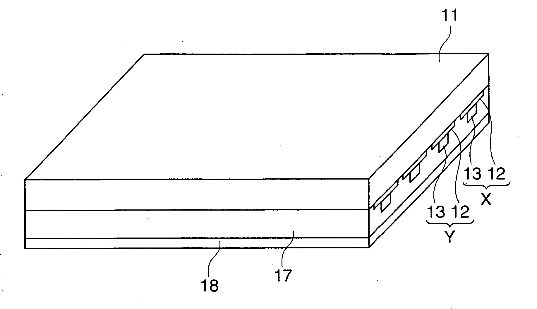
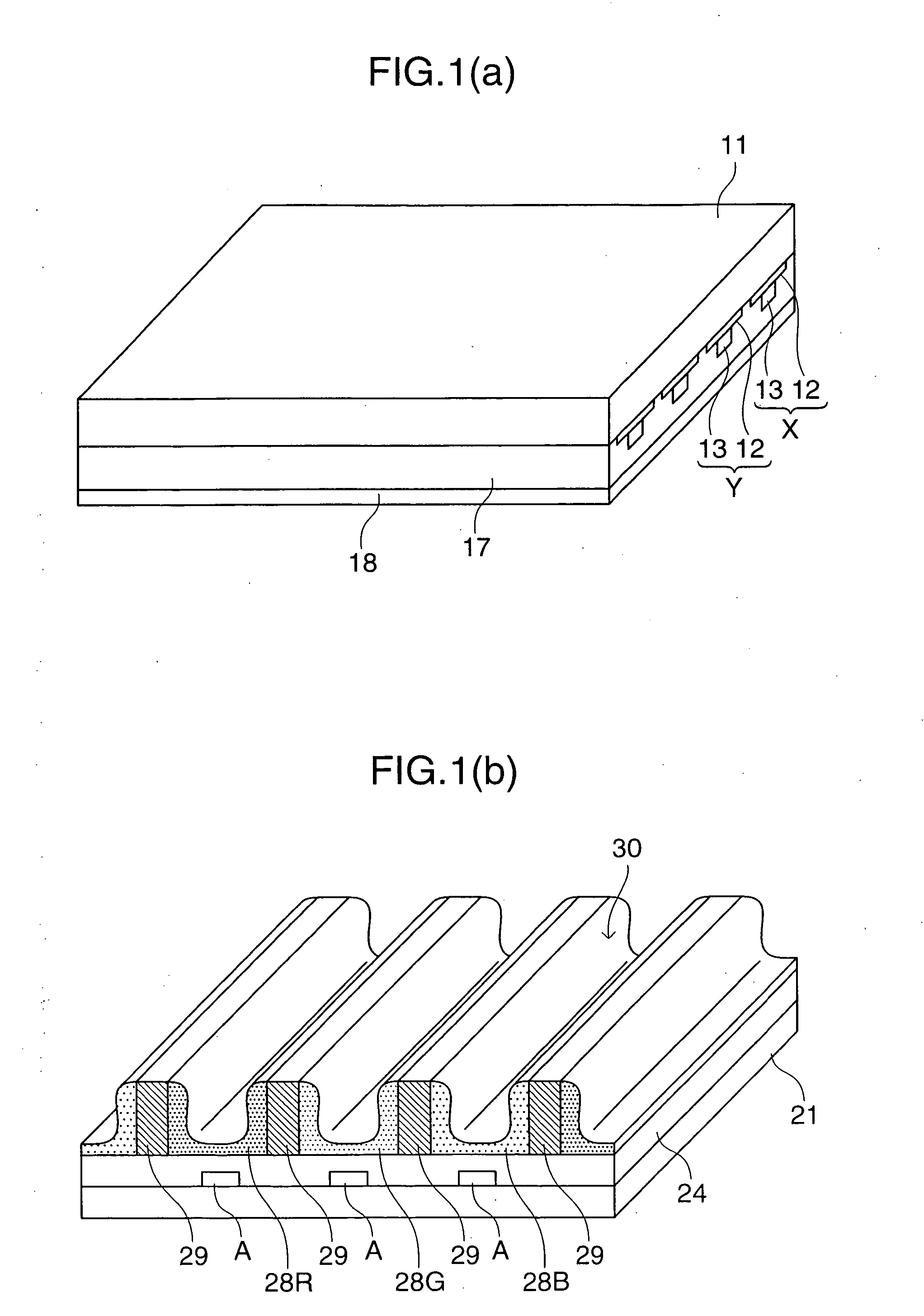
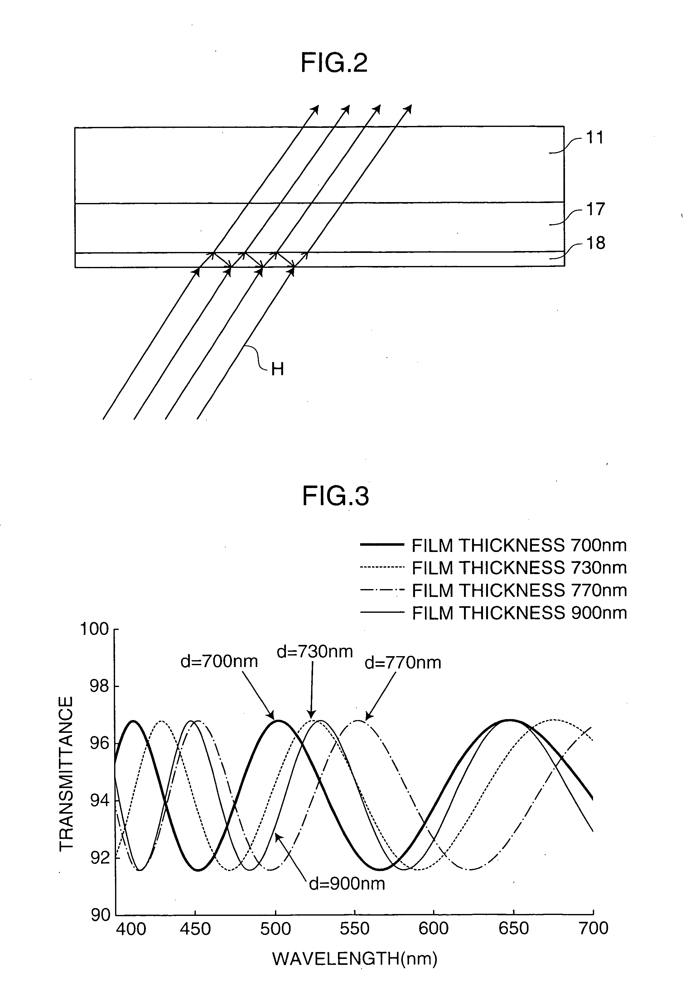
[0024] In the present invention, the index of refraction means the ratio c / v of light velocity c in a vacuum to light velocity (phase velocity) v in a medium. Accordingly, the index of refraction of a dielectric layer means the ratio of light velocity in a vacuum to light velocity in the dielectric layer, and the index of refraction of a protective film means the ratio of light velocity in a vacuum to light velocity in the protective film.

[0025] In the present invention, the index of refraction is not defined in size, but rather, the difference in the index of refraction is defined. The difference in the index of refraction between a dielectric layer and a protective film is difference in index of refraction Δn=|n−n1|, where n is the index of refraction of the dielectric layer and n1 is the index of refraction of the protective film. Accordingly, either the index of refraction of the dielectric layer or the index of refraction of the protective film may be greater.

[0026] In the pr...


PUM


Abstract

An AC type plasma display panel includes a front substrate and a rear substrate defining a discharge space therebetween, electrodes formed on the inner surface of the front substrate, a dielectric layer covering the electrodes, and a protective film covering the dielectric layer. The difference in the index of refraction between the dielectric layer and the protective film is not greater than 0.20. According to the present invention, lack of uniformity due to interference is lessened by taking the difference in the index of refraction between a dielectric layer and a protective film into consideration.

Description

CROSS-REFERENCE TO RELATED APPLICATION [0001] This application is related to Japanese Patent Application No. 2004-304499 filed on Oct. 19, 2004, on the basis of which priority is claimed under 35 USC §119, the disclosure of this application being incorporated by reference in its entirety. BACKGROUNF OF THE INVENTION [0002] 1. Field of the Invention [0003] The present invention relates to a plasma display panel (hereinafter referred to as “PDP”) and a manufacturing method for the same, and in particular, to a PDP where lack of uniformity in the display is lessened, and a manufacturing method for the same. [0004] 2. Description of the Related Art [0005] An AC type 3-electrode surface discharge style PDP is known as a conventional PDP. In this PDP, a great number of display electrodes which allow for surface discharge are provided on the inner surface of a substrate on the front side (display surface side) in a lateral direction, while a great number of address electrodes for selecting...

Claims


Application Information

Patent Timeline
IPC IPC(8): H01J17/49H01J9/02H01J11/12H01J11/22H01J11/24H01J11/26H01J11/34H01J11/38H01J11/40
CPCH01J9/02H01J11/12H01J11/38H01J11/40
Inventor KAWASAKI, TATSUHIKO
Owner FUJITSU HITACHI PLASMA DISPLAY LTD
Why Eureka
Try Eureka