Current source circuit

a current source circuit and current source technology, applied in the direction of automatic control, process and machine control, instruments, etc., can solve the problems of unnecessary power consumption and continue, and achieve the effect of preventing steady current consumption, reducing the power consumption of the overall circuit, and eliminating unnecessary power consumption

Inactive Publication Date: 2006-04-27
PANASONIC CORP
View PDF13 Cites 21 Cited by
  • Summary
  • Abstract
  • Description
  • Claims
  • Application Information

AI Technical Summary

Benefits of technology

[0014] The present invention is devised to solve the conventional problem. An object of the present invention is to provide a current source circuit which can eliminate unnecessary power consumption after the start of a bias circuit and reduce the power consumption of the overall circuit.
[0019] As described above, after the start of the bias circuit, the startup circuit is isolated from the bias circuit according to the bias voltage generated on the isolating voltage node from the bias circuit to the startup circuit, and steady current consumption can be prevented in the startup circuit.
[0020] Therefore, it is possible to eliminate unnecessary power consumption after the start of the bias circuit, thereby further reducing the power consumption of the overall circuit.

Problems solved by technology

Thus, unnecessary power consumption continues in the startup circuit 60, which is a problem in achieving low power consumption in the overall circuit.

Method used


Image

  • Current source circuit
  • Current source circuit
  • Current source circuit

Examples


embodiment 1

[0027] A current source circuit will be discussed below according to Embodiment 1 of the present invention.

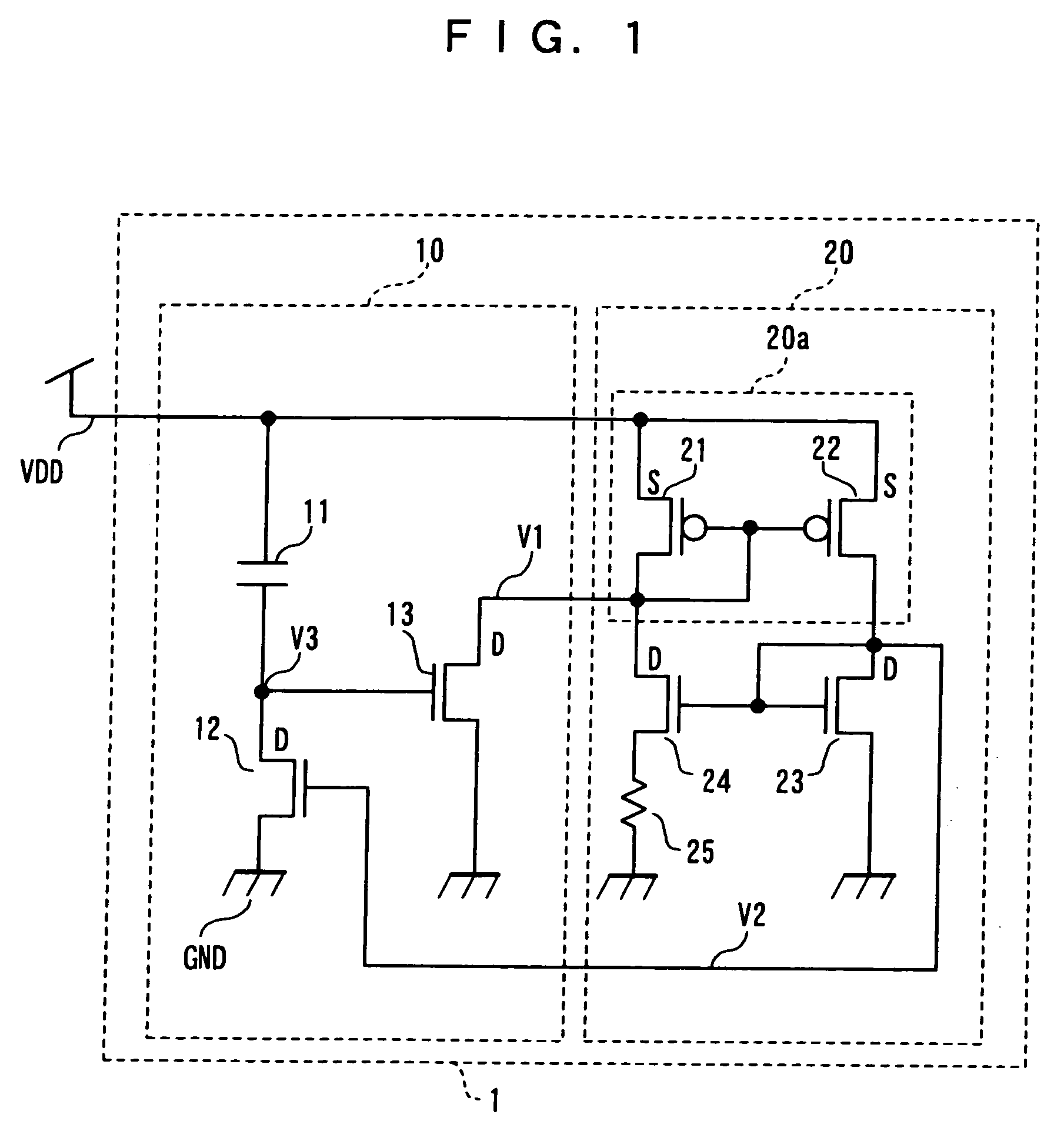
[0028]FIG. 1 is a circuit diagram showing the configuration of the current source circuit according to Embodiment 1. In FIG. 1, in the basic configuration of the current source circuit 1 of the present embodiment, a startup circuit 10 and a bias circuit 20 are connected to each other. The startup circuit 10 operates between a power supply VDD and ground GND when the power supply VDD is turned on, and the bias circuit 20 starts to pass current when the startup circuit 10 operates.

[0029] The startup circuit 10 is comprised of a capacitor 11 connected between the power supply VDD and a control voltage node V3, an NMOS transistor 12 having a drain connected to the control voltage node V3, a source connected to the ground GND, and a gate connected to an isolating voltage node V2 from the bias circuit 20, and an NMOS transistor 13 having a gate connected to the control voltage node...

embodiment 2

[0037] A current source circuit will be discussed below according to Embodiment 2 of the present invention.

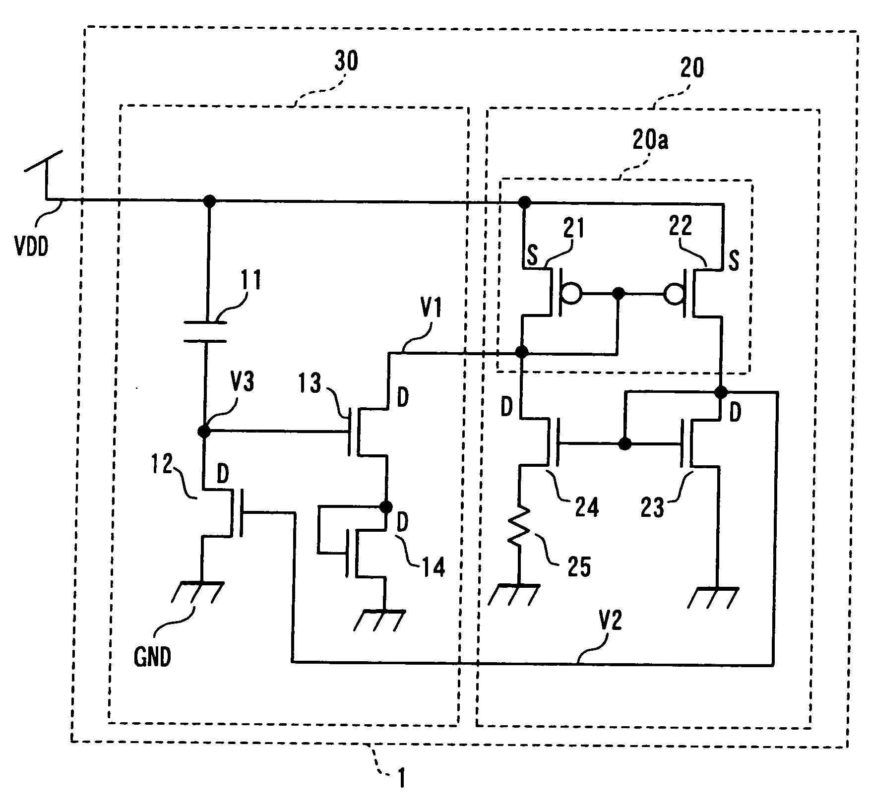
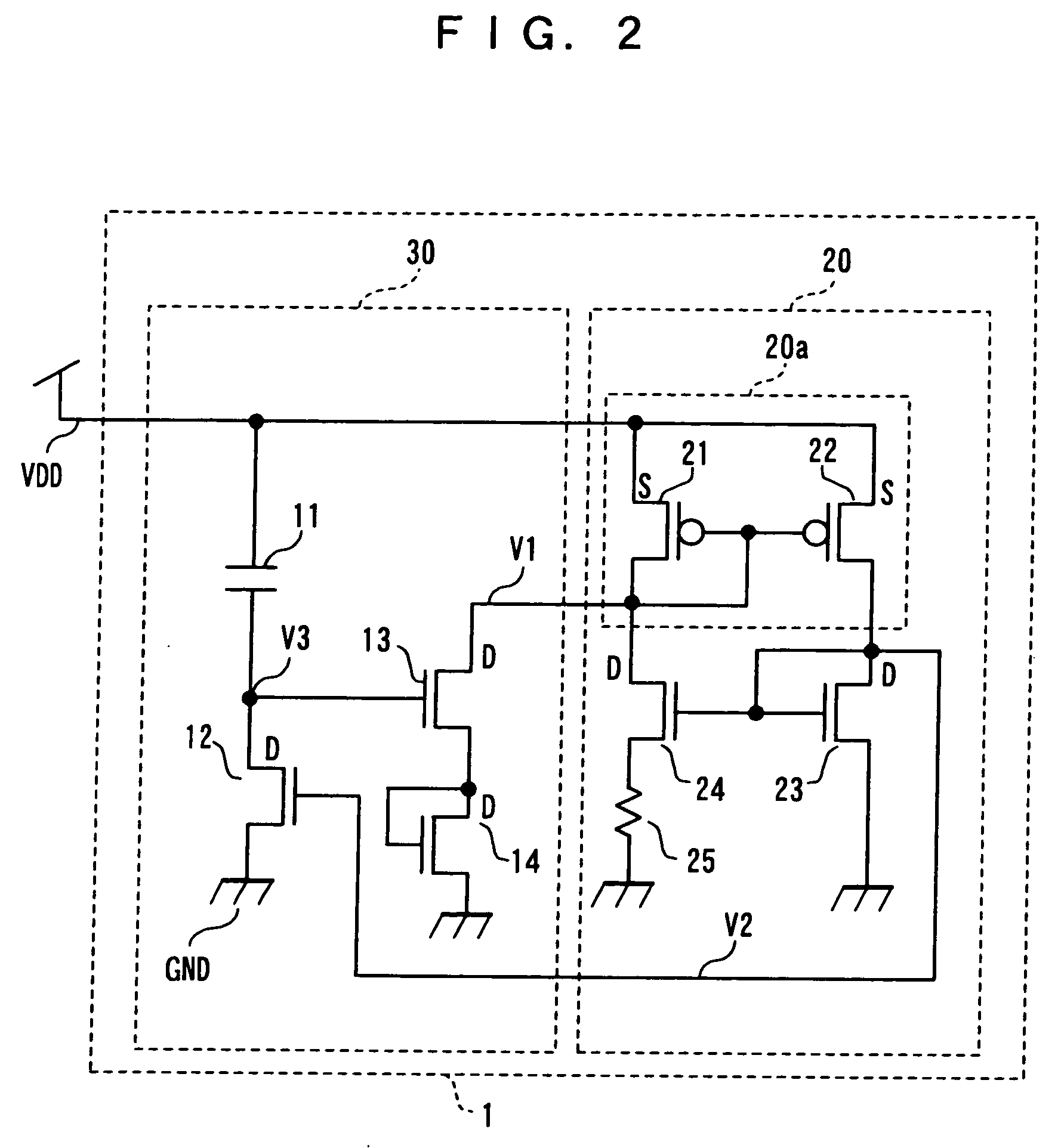
[0038]FIG. 2 is a circuit diagram showing the configuration of the current source circuit according to Embodiment 2. In FIG. 2, in the basic configuration of the current source circuit 1 of Embodiment 2, a startup circuit 30 and a bias circuit 20 are connected to each other. The startup circuit 30 operates between a power supply VDD and ground GND when the power supply VDD is turned on, and the bias circuit 20 starts to pass current when the startup circuit 30 operates.

[0039] The startup circuit 30 is comprised of a capacitor 11 connected between the power supply VDD and a control voltage node V3, an NMOS transistor 12 having a drain connected to the control voltage node V3, a source connected to the ground GND, and a gate connected to an isolating voltage node V2 from the bias circuit 20, an NMOS transistor 13 having a gate connected to the control voltage node V3 and a drai...

embodiment 3

[0044] A current source circuit will be discussed below according to Embodiment 3 of the present invention.

[0045]FIG. 3 is a circuit diagram showing the configuration of the current source circuit according to Embodiment 3. In FIG. 3, in the basic configuration of the current source circuit 1 of Embodiment 3, a startup circuit 40 and a bias circuit 20 are connected to each other. The startup circuit 40 operates between a power supply VDD and ground GND when the power supply VDD is turned on, and the bias circuit 20 starts to pass current when the startup circuit 40 operates.

[0046] The startup circuit 40 is comprised of a PMOS transistor 41 having a source connected to the power supply VDD and having a gate and a drain connected to a shift voltage node V4, a capacitor 42 connected between the shift voltage node V4 and the ground GND, a capacitor 43 having one end connected to the power supply VDD, an NMOS transistor 44 having a drain connected to the other end of the capacitor 43, ...


PUM


Abstract

According to the present invention, after a bias circuit (20) starts, a startup circuit (10) is isolated from the bias circuit (20) according to a bias voltage generated on an isolating voltage node (V2) from the bias circuit (20) to the startup circuit (10), and steady current consumption can be prevented in the startup circuit (10).

Description

FIELD OF THE INVENTION [0001] The present invention relates to a current source circuit in which a startup circuit operates to start a bias circuit at power-on for starting a device. BACKGROUND OF THE INVENTION [0002] Conventionally, in a semiconductor integrated circuit device or the like including a plurality of digital circuits and analog circuits which form various functional blocks, a startup circuit operates at power-on for starting the device. To supply bias voltage to the various functional blocks after the operation, a current source circuit for starting a bias circuit for generating bias voltage is externally connected or included. [0003] Such a conventional current source circuit will be discussed below in accordance with the accompanying drawings. [0004] For example, FIG. 5 is a circuit diagram showing the configuration of a conventional current source circuit disclosed in “CMOS Circuit Design, Layout, and Simulation” by R. Jacob Baker, Harry W. Li, David E. Boyce, John ...

Claims


Application Information

Patent Timeline
Patent Type & Authority Applications(United States)
IPC IPC(8): G05F1/10
CPCG05F3/205G05F3/242G05F3/262
Inventor INOUE, ATSUO
Owner PANASONIC CORP
Why Eureka
Try Eureka