
One chip camera with color sensing capability and high limiting resolution

a color sensing and high-limiting resolution technology, applied in the field of one-chip low-light level imaging devices, can solve the problem that pixels are incapable of discriminating between colors, and achieve the effects of improving color performance, high spatial frequency resolution, and high resolution

Active Publication Date: 2006-04-27
BALL AEROSPACE & TECHNOLOGIES
View PDF26 Cites 34 Cited by
  • Summary
  • Abstract
  • Description
  • Claims
  • Application Information

AI Technical Summary

Benefits of technology

"The present invention provides a one chip, low light level imaging device with panchromatic pixels and a small proportion of color sensitive pixels. The panchromatic pixels are sensitive to light across the full spectral range of the image sensor, while the color sensitive pixels provide color information. The image sensor has a high spatial sensing frequency for high resolution and high sensitivity. The panchromatic pixels can be used for luminance or brightness assessment, while the color information from the color sensitive pixels is only used for luminance or brightness assessment. The image sensor can also include a global near infrared blocking filter to improve color performance in low light environments and reduce noise. Additionally, the image sensor can include effective opaque pixels to mitigate the effects of charge diffusion."

Problems solved by technology

Accordingly, these pixels are incapable of discriminating between colors, or providing information for discriminating between colors, and are instead panchromatic.

Method used


Image

  • One chip camera with color sensing capability and high limiting resolution
  • One chip camera with color sensing capability and high limiting resolution
  • One chip camera with color sensing capability and high limiting resolution

Examples


Embodiment Construction

[0046] According to the present invention, a one chip, low light level color imaging device or camera is provided.

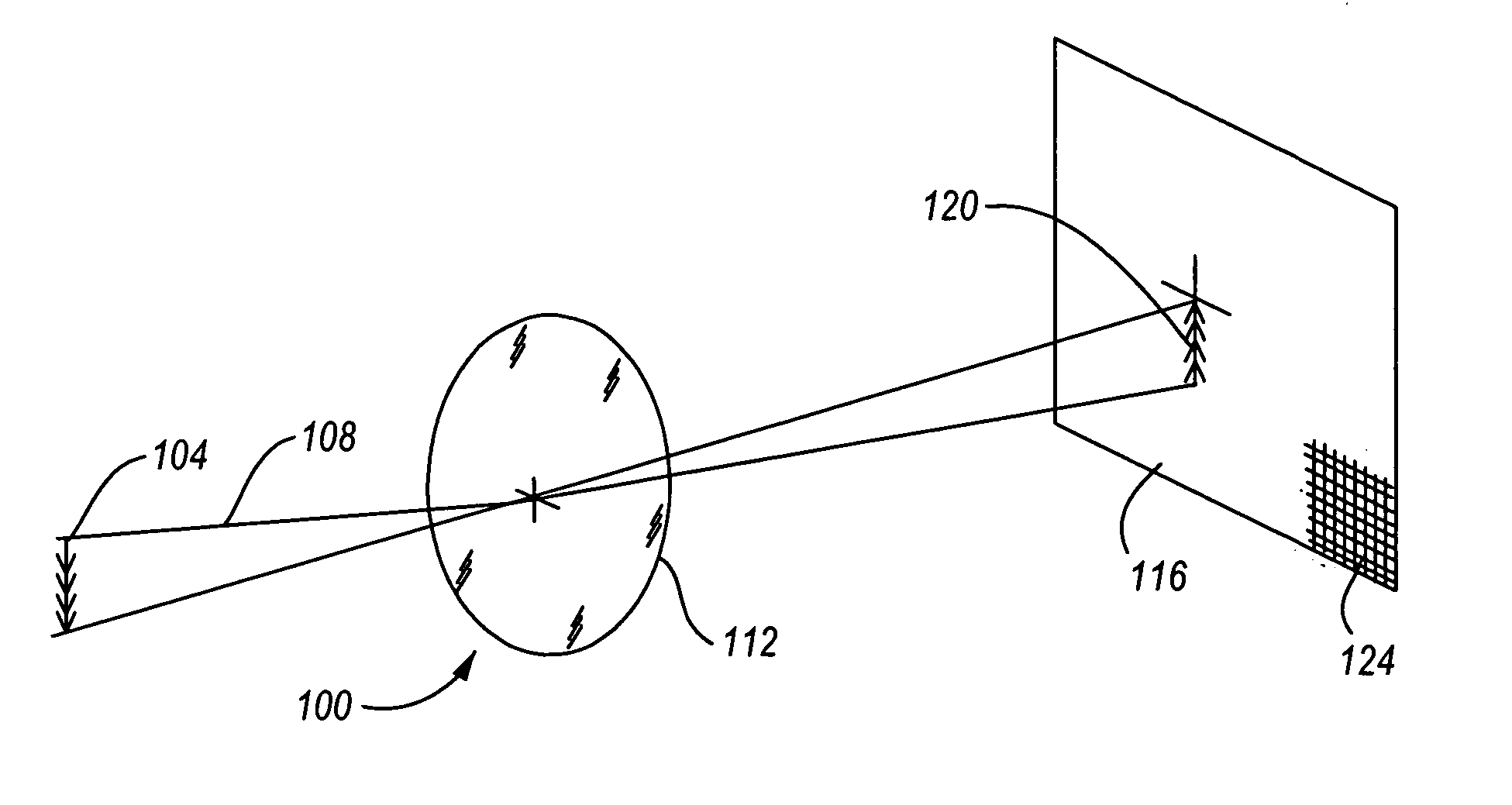
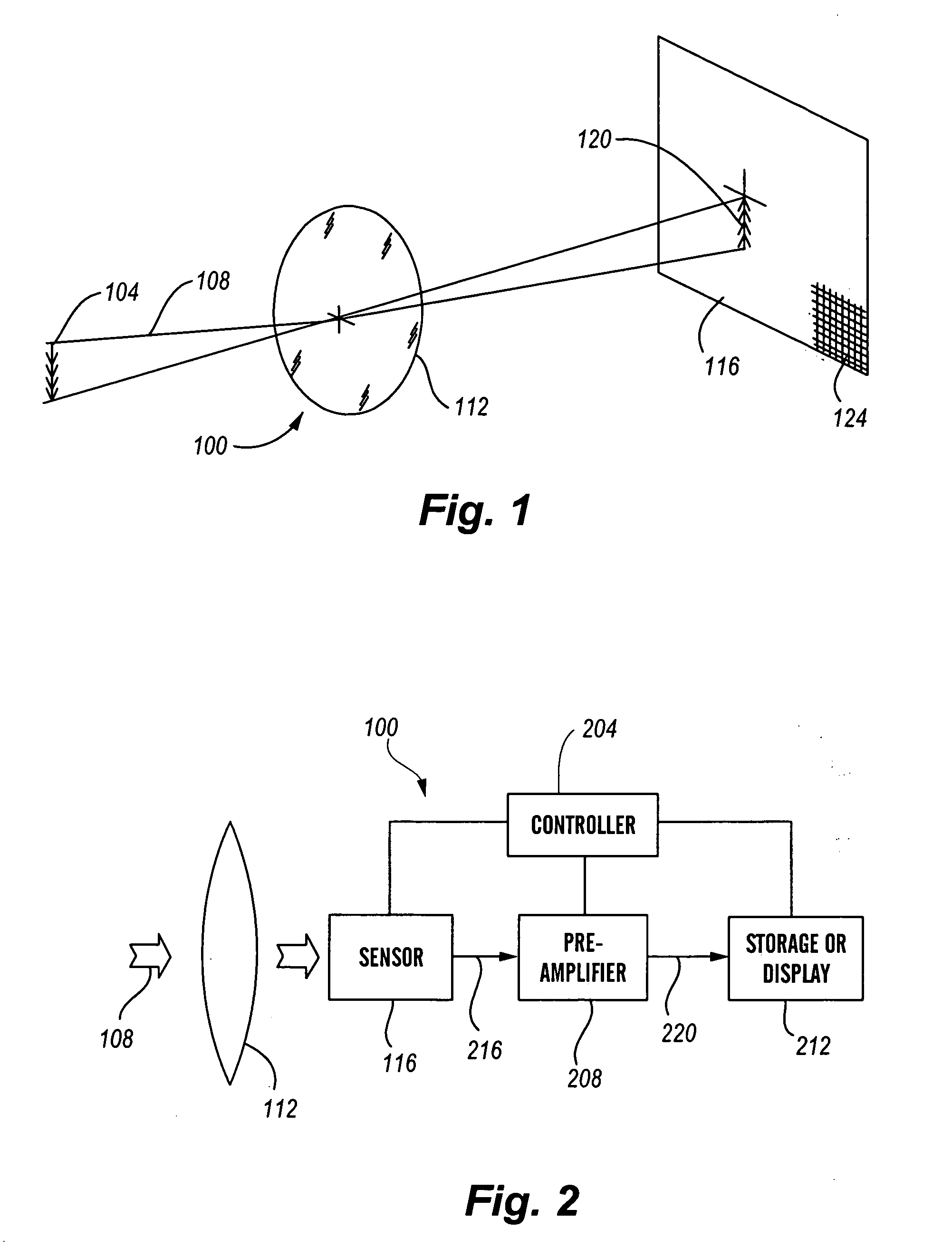
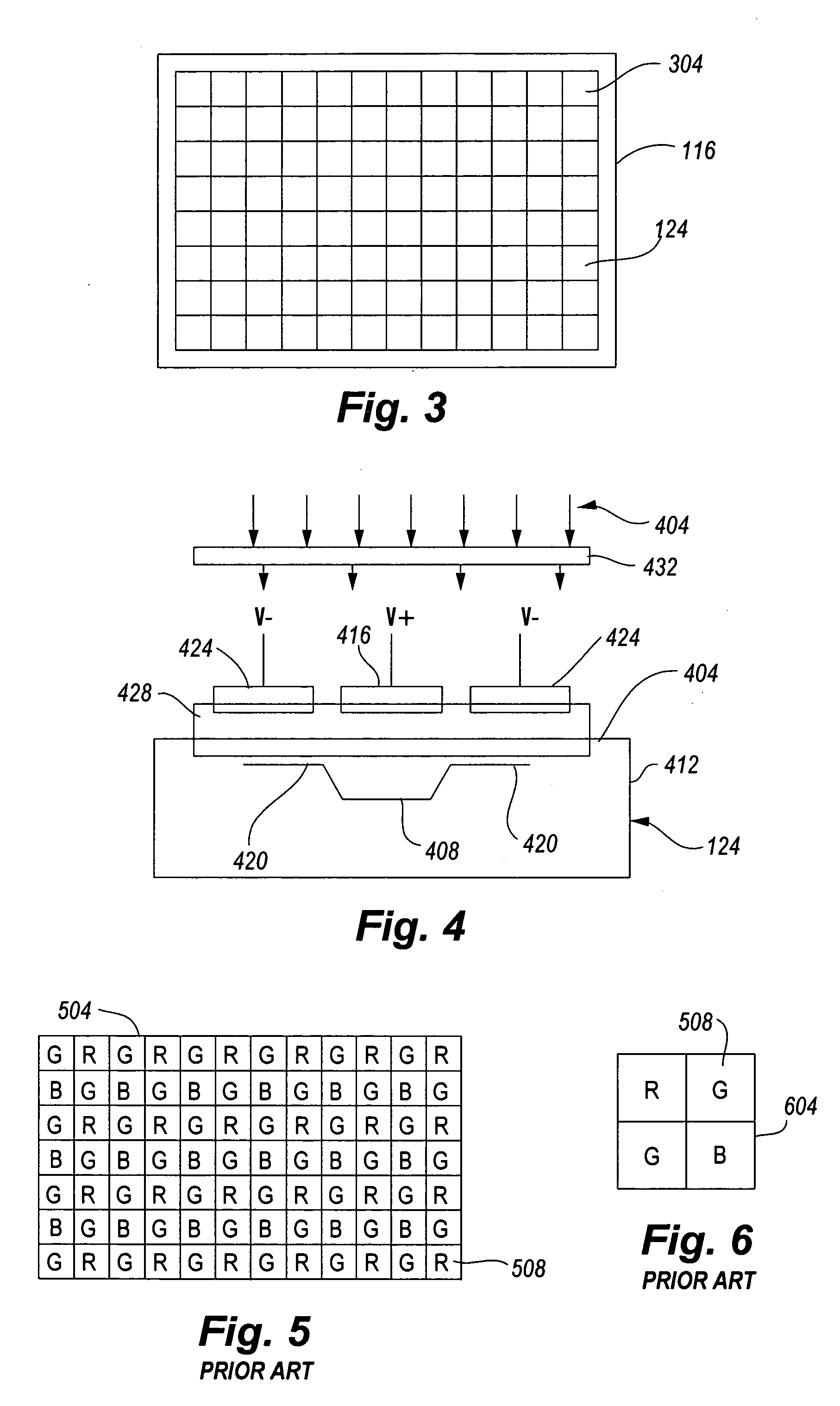
[0047] In FIG. 1, a digital imaging device 100 configuration suitable for use in connection with the present invention is illustrated. As shown in FIG. 1, an object 104 reflects light 108 that is focused by a lens or lens system 112 onto an image sensor 116 as an image object 120. The image sensor 116 is comprised of a plurality of photosensitive elements or pixels 124. The pixels 124 are distributed over the surface of the image sensor 116 in a two-dimensional array. The pixels 124 generally convert the light focused onto the surface of the image sensor 116 by the lens 112 (i.e. the image object 120) into electronic signals.

[0048] In a conventional color imaging device, each of the pixels 124 of the image sensor 116 receive light within one of three overlapping frequency bands. The relative intensity of the light received by individual pixels 124 included in a group o...


PUM


Abstract

A high sensitivity, single chip, low light level imaging device is provided. The imaging device of the present invention utilizes sparse color sampling, to maximize the luminance information gathered. In particular, color information is gathered by a small proportion of the pixels included in an image sensor, while the remaining pixels operate at full spectrum sensitivity. The present invention allows the correct hue of objects to be determined, while providing high sensitivity to available luminance information in a scene. The imaging device can include a global near infrared blocking filter that can be selectively placed in the optical path of the device. In addition or alternatively, opaque pixels may be included in the image sensor to correct for errors caused by charge diffusion.

Description

CROSS REFERENCE TO RELATED APPLICATIONS [0001] This application is a Continuation-In-Part of U.S. patent application Ser. No. 10 / 142,320, filed May 8, 2002, the entire disclosure of which is hereby incorporated herein by reference.FIELD OF THE INVENTION [0002] The present invention relates to one chip low light level imaging devices. In particular, the present invention relates to electronic imaging devices that include a number of pixels, the majority of which are capable of sensing light at wavelengths extending into the near infrared. BACKGROUND OF THE INVENTION [0003] Low light level imaging devices are useful in a wide variety of applications. For example, low light level imaging devices are useful in nighttime surveillance activities. In low light level conditions, it is important for sensors to take advantage of every available photon. Approaches to providing human perceptible images in low light conditions have included the use of image intensifiers. Other approaches to prov...

Claims


Application Information

Patent Timeline
Patent Type & Authority Applications(United States)
IPC IPC(8): H04N5/76H04N5/225H01L27/148H04N9/03H04N23/12
CPCH04N5/332H04N9/045H04N2209/045H04N2209/047H04N23/11H04N23/843H04N25/134
Inventor FRAME, WAYNE W.HEIM, GERALD B.
Owner BALL AEROSPACE & TECHNOLOGIES
Learn More