Multi-layer printed circuit with low noise
- Summary
- Abstract
- Description
- Claims
- Application Information
AI Technical Summary
Benefits of technology
Problems solved by technology
Method used
Image
Examples
Embodiment Construction
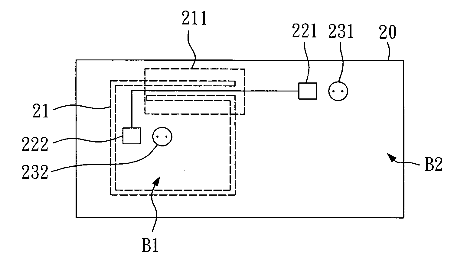
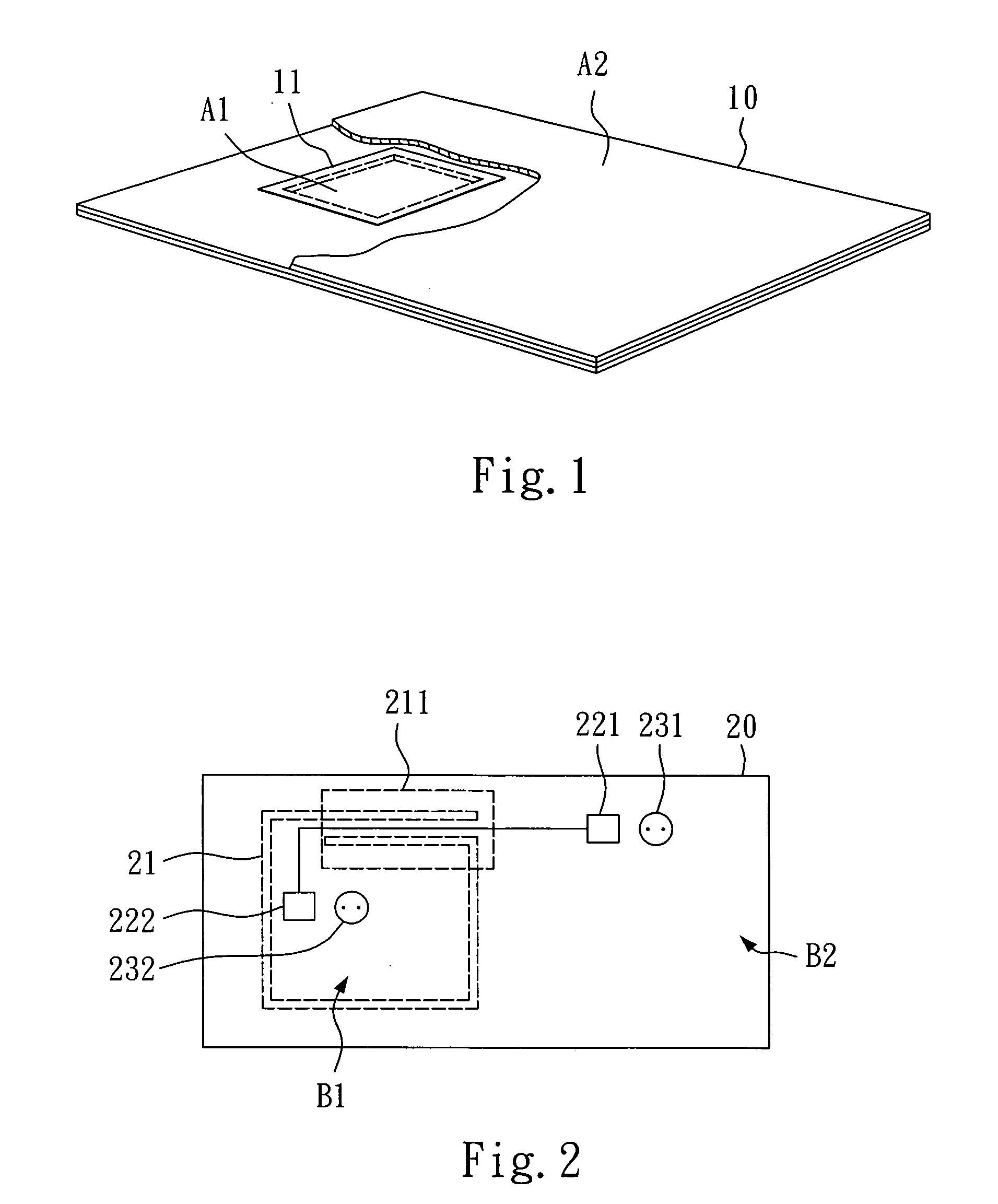
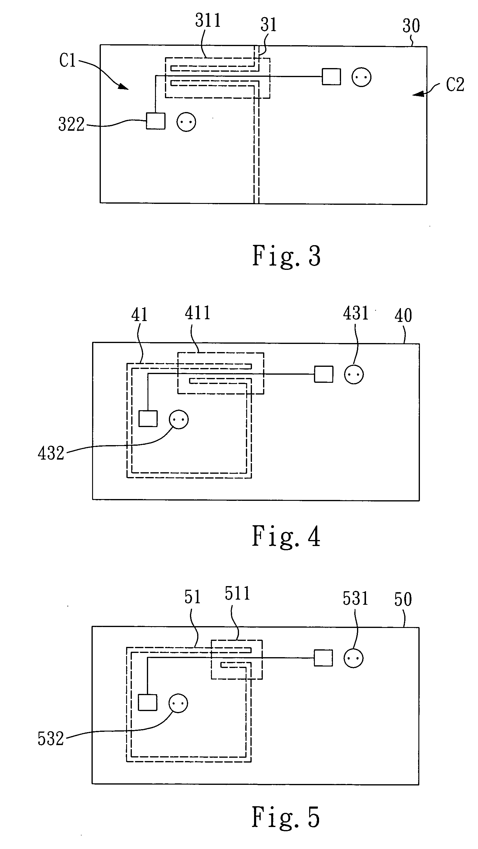
[0020]FIG. 2 is shown a schematic drawing of a printed circuit board of a first embodiment according to the present invention. A printed circuit 20 has a component layer, with a power layer and a ground layer (not shown) that are respectively placed above and below it. Many digital electronic components 221 and many analog electronic components 222 are placed on the printed circuit board 20. In this embodiment, an isolation line 21 is used to surround an analog electronic component area B1 to form an open rectangle and to extend into the analog electronic components area B1 to form a long neck line 211. The rest of the area of the printed circuit board 20 is a digital electronic components area B2. Signal lines for connecting the digital electronic components 221 and the analog electronic components 222 pass over the long neck line 211. This design can reduce noise interference between the two areas. Moreover, the electromagnetic radiation from the printed circuit board 20 can be re...
PUM
 Abstract
Description
Claims
Application Information


