Integrated circuit device and imaging apparatus using integrated circuit device

Active Publication Date: 2009-06-25
CANON KK
View PDF3 Cites 8 Cited by
  • Summary
  • Abstract
  • Description
  • Claims
  • Application Information

AI Technical Summary

Benefits of technology

[0007]However, according to the configuration disclosed in U.S. Pat. No. 6,456,270, if the number of the signal processing circuits provided in a semiconductor integrated circuit device increases, then the wiring resistances of the bias current setting lines and the power supply lines and the potential gradients generated by the currents flowing through the bias current setting lines and the power supply lines increase. Consequently, a gradient is caused between the operation biases to be supplied to the amplifier circuits of the respective signal processin

Problems solved by technology

Because the output gradient is conspicuous in an image signal, the output gradient rem

Method used


Image

  • Integrated circuit device and imaging apparatus using integrated circuit device
  • Integrated circuit device and imaging apparatus using integrated circuit device
  • Integrated circuit device and imaging apparatus using integrated circuit device

Examples


first embodiment

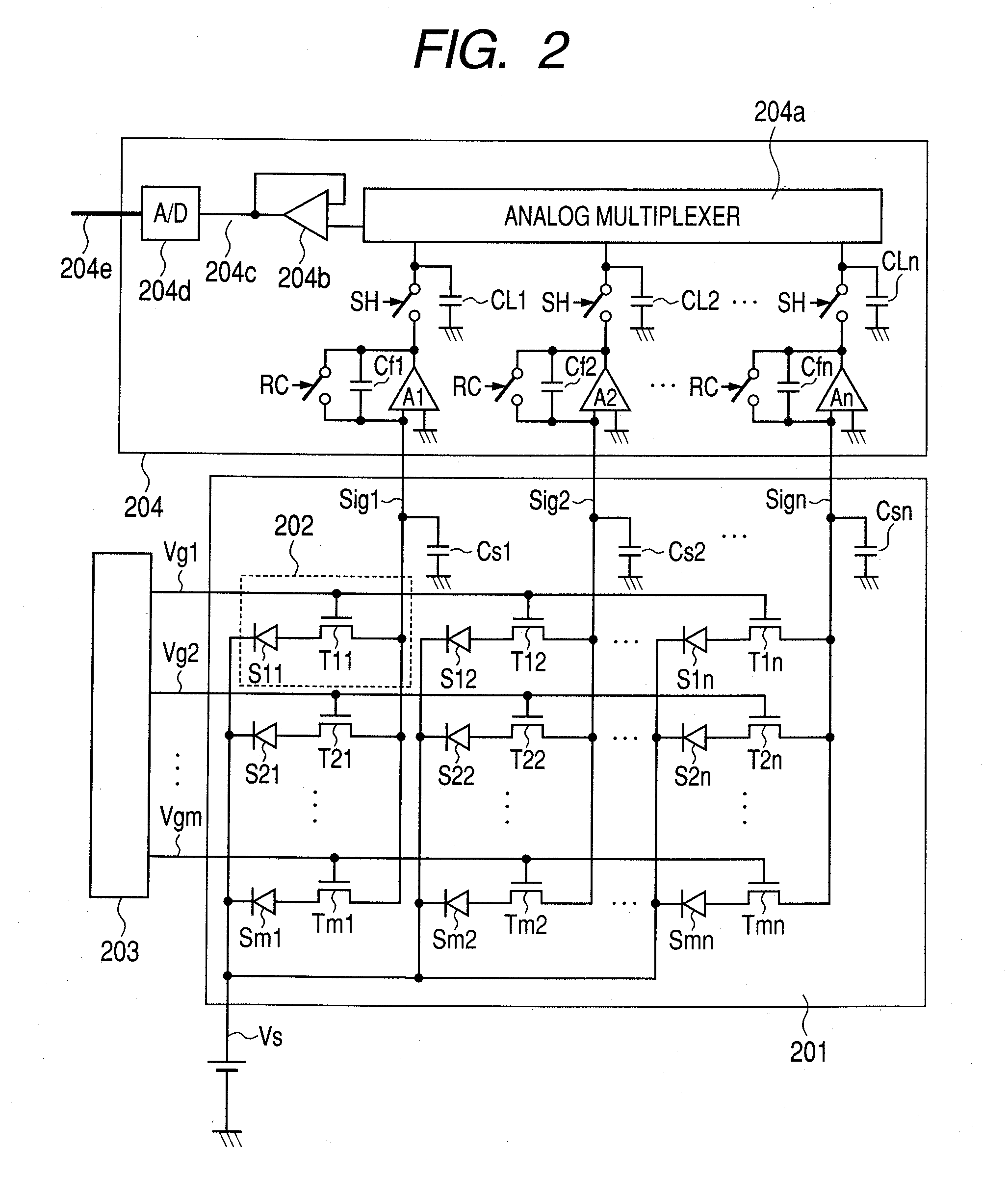
[0025]First, the whole configuration of an imaging apparatus of the present invention will be described with reference to FIG. 2. FIG. 2 illustrates a schematic equivalent circuit diagram of an imaging apparatus of a first embodiment of the present invention.

[0026]A detector 201 and a drive circuit 203 are connected to each other with m (m is a positive integer) drive lines Vg1-Vgm. Moreover, the detector 201 and a semiconductor integrated circuit device 204 are connected to each other with n (n is a positive integer) signal lines Sig1-Sign.

[0027]The detector 201 includes a plurality of two-dimensionally arranged pixels 202 each including each of conversion elements S11-Smn, which include photoelectric conversion elements, such as PIN type photodiodes, and each of switching elements T11-Tmn, which are made of thin film transistors (TFTs). That is, m×n pixels 202 are arranged in a matrix in the detector 201. The detector 201 is, for example, a flat panel type detector configured of a...

second embodiment

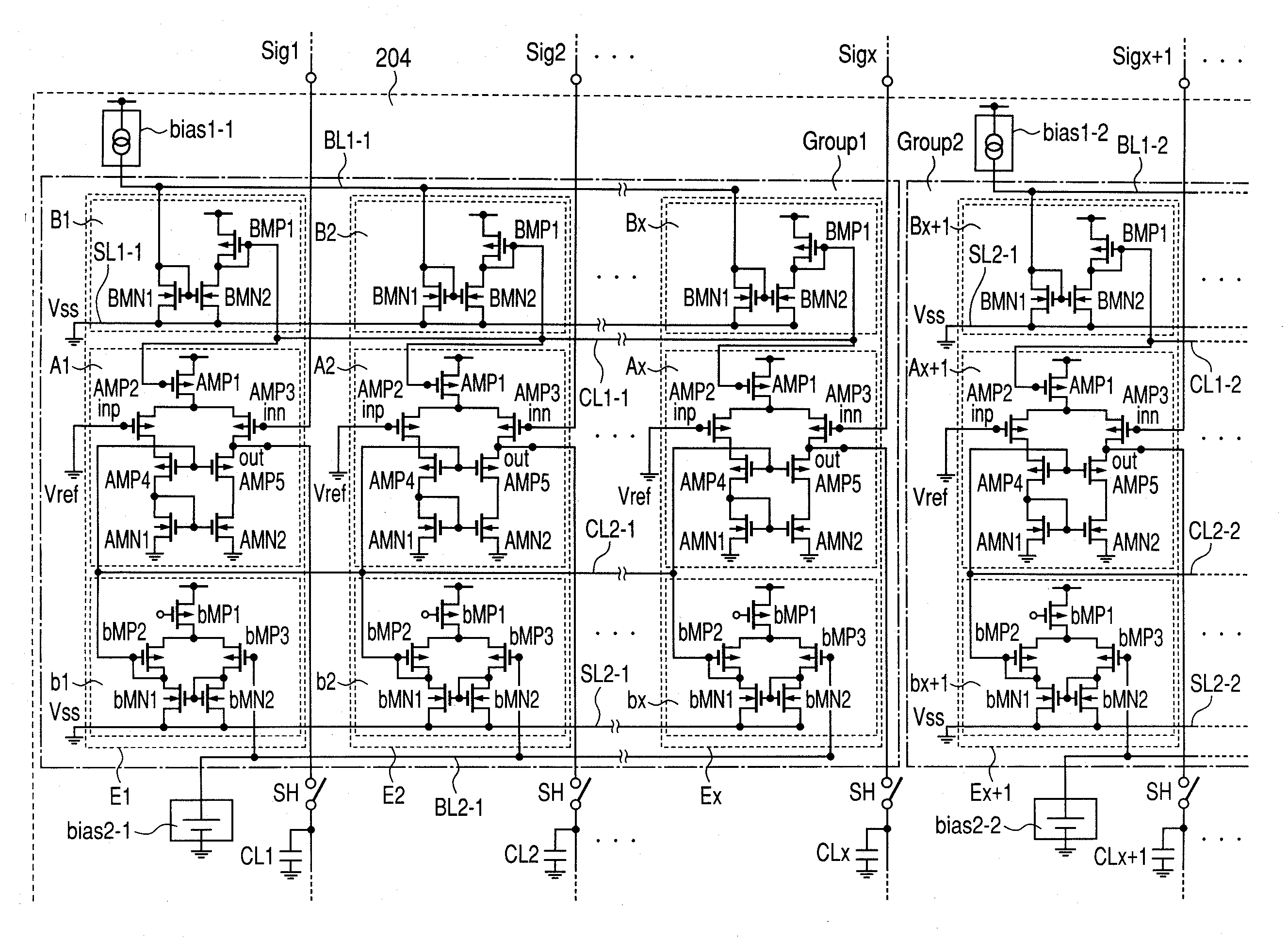
[0047]The semiconductor integrated circuit device 204 according to the present embodiment will be described with reference to FIG. 7. Incidentally, the same components as those of the first embodiment are denoted by the same reference numerals or signs, and their descriptions are omitted. FIG. 7 is a schematic equivalent circuit diagram of a part of one of the semiconductor integrated circuit device 204 according to the present embodiment.

[0048]The present embodiment differs from the first embodiment in that the first group thereof includes x signal processing circuits E1 to E(2x−1) corresponding to the signal lines Sig1 to Sig(2x−1) of odd columns, and in that the second group thereof includes x signal processing circuits E2 to E2x corresponding to the signal lines Sig2 to Sig2x of even columns. That is, in the present embodiment, both of the signal processing circuits corresponding to predetermined signal lines among the plurality of signal lines Sig1 to Sig2x included in the dete...

third embodiment

[0050]Next, a radiation imaging system using a radiation imaging apparatus, which is an imaging apparatus according to the present invention, will be described with reference to FIG. 8.

[0051]As illustrated in FIG. 8, an X-ray 6060 generated by an X-ray generating apparatus 6050, which is a radiation source, penetrates through the breast 6062 of a patient or subject 6061, and enters a radiation imaging apparatus 6040. The entered X-ray 6060 includes the information of the inside of the body of the patient 6061. The phosphor of the radiation imaging apparatus 6040 emits a light correspondingly to the incidence of the X-ray 6060, and the emitted light is photoelectrically converted. Electric information can be thus obtained. The information is converted into digital information, and is subjected to image processing by an image processor 6070, which is a signal processing unit. The processed image can be observed on a display 6080, which is a display unit in a control room.

[0052]Moreove...


PUM


Abstract

An integrated circuit device of the present invention includes a plurality of signal processing circuits classified into a plurality of groups, each signal processing circuit including an amplifier circuit for amplifying an input electric signal and a bias circuit having an input terminal connected electrically to a bias source and supplying a bias input terminal of the amplifier circuit with an operation bias for an amplifying operation of the amplifier circuit; and a plurality of connection wirings arranged each for each of the groups separately, such that the input terminals of the bias circuits of the signal processing circuits in one of the groups are commonly connected through the connection wirings. This provides an integrated circuit device suppressing the lowering of an image quality in consideration of enabling lower power consumption, a low noise characteristic, and high integration, and an imaging apparatus using the integrated circuit.

Description

BACKGROUND OF THE INVENTION[0001]1. Field of the Invention[0002]The present invention relates to a semiconductor integrated circuit device including a signal processing circuit for performing the signal processing of an imaging apparatus, an imaging apparatus including the semiconductor integrated circuit device, and a radiation imaging apparatus and radiation imaging system that use the semiconductor integrated circuit device. Incidentally, in the present description, it is supposed that a term of radiation includes an electromagnetic wave, an X-ray, an α-ray, a β-ray, a γ-ray, and the like.[0003]2. Description of the Related Art[0004]In an imaging apparatus including a detector including a plurality of pixels arranged in a matrix, an image signal from the detector is processed by using a semiconductor integrated circuit device including a plurality of signal processing circuits arranged in an array, which signal processing circuits process a signal output from the detector by the ...

Claims


Application Information

Patent Timeline
IPC IPC(8): H01L27/00H03F1/00H03F3/04H03F3/16
CPCH03F3/08H04N5/32H04N5/378H04N5/3742H04N5/357H04N25/60H04N25/767H04N25/75
Inventor KOBAYASHI, DAISUKEYOSHIDA, DAISUKE
Owner CANON KK
Why Eureka
Try Eureka