Trench MOSFET with deposited oxide

Active Publication Date: 2006-05-04
INFINEON TECH AMERICAS
View PDF4 Cites 13 Cited by
  • Summary
  • Abstract
  • Description
  • Claims
  • Application Information

AI Technical Summary

Benefits of technology

[0009] According to another aspect of the present invention, a device according to the present invention includes a field relief trench, a field oxide body having a recess, and a T-shaped electrode received at least

Problems solved by technology

It is well known that a high electric field at the bottom of the trench can compromise the integrity of the device.
Oxidation, however, is time consuming, which is costly.
In addition,

Method used


Image

  • Trench MOSFET with deposited oxide
  • Trench MOSFET with deposited oxide
  • Trench MOSFET with deposited oxide

Examples


Example

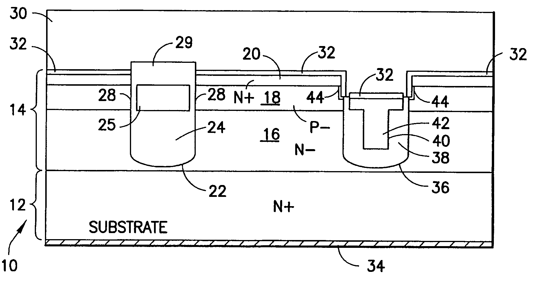
[0016] Referring to FIG. 1, a power semiconductor device according to the present invention includes semiconductor body 10. Semiconductor body 10 preferably includes semiconductor substrate 12, which may be a float-zone type, single crystal, silicon, and an epitaxially grown semiconductor body 14, for example, epitaxially formed silicon, formed over substrate 12. Epitaxially grown semiconductor body 14 includes drift region 16, channel region (sometimes referred to as body region) 18, and conductive region 20 over channel region 18. As is well known in the art, drift region 16, and conductive region 20 are of one conductivity, while channel region 18 is of another, opposite conductivity. Thus, when drift region 16, and conductive region 20 are of N-type conductivity, channel region 18 is of the P-type variety, and when drift region 16, and conductive region 20 are of P-type conductivity, channel region 18 is of the N-type variety.

[0017] A power semiconductor device according to the...


PUM


Abstract

A trench type power semiconductor device which includes deposited rather than grown oxide in the trenches for the electrical isolation of electrodes disposed inside the trenches from the semiconductor body.

Description

RELATED APPLICATION [0001] This application is based on and claims benefit of U.S. Provisional Application Ser. No. 60 / 623,679, filed on Oct. 29, 2004, entitled Trench MOSFET Structures Using Deposited Oxide With Spacers, to which a claim of priority is hereby made and the disclosure of which is incorporated by reference.BACKGROUND OF THE INVENTION [0002] The present invention relates to semiconductor devices and more particularly to trench type power semiconductor devices. [0003] A typical trench type power semiconductor device includes a gate structure, which is supported inside a trench. The gate structure includes a conductive gate electrode insulated from the semiconductor body of the device by an insulation body, which is typically silicon dioxide. [0004] It is well known that a high electric field at the bottom of the trench can compromise the integrity of the device. To overcome this problem, a thick oxide is formed at the bottom of the trench below the gate electrode. [0005...

Claims


Application Information

Patent Timeline
IPC IPC(8): H01L29/94
CPCH01L29/407H01L29/42368H01L29/66734H01L29/7811H01L29/7813
Inventor MONTGOMERY, ROBERT
Owner INFINEON TECH AMERICAS
Why Eureka
Try Eureka