Top and sidewall bridged interconnect structure and method

a technology of interconnect structure and top and sidewall, which is applied in the direction of semiconductor devices, semiconductor/solid-state device details, electrical devices, etc., can solve the problems of difficult effective interconnection of devices, and achieve the effect of improving performance, efficient and effective connection

Active Publication Date: 2006-05-04
TAIWAN SEMICON MFG CO LTD
View PDF3 Cites 97 Cited by
  • Summary
  • Abstract
  • Description
  • Claims
  • Application Information

AI Technical Summary

Benefits of technology

[0010] The invention provides an interconnect structure with enhanced performance, and a method for fabricating the same. The invention realizes the foregoing objects by employing a bridging conductor layer formed upon a contact region within a semiconductor substrate and bridging to a sidewall and a top surface of an interconnect patterned over the contact region of the semiconductor substrate. In particular, by bridging to the top surface of the interconnect, the bridging conductor layer provides an efficient and effective connection between the active region and the interconnect.

Problems solved by technology

As semiconductor product integration levels increase, effective interconnection of devices often becomes difficult due to lithographic resolution and overlay considerations when forming patterned conductor layers.

Method used


Image

  • Top and sidewall bridged interconnect structure and method
  • Top and sidewall bridged interconnect structure and method
  • Top and sidewall bridged interconnect structure and method

Examples


Embodiment Construction

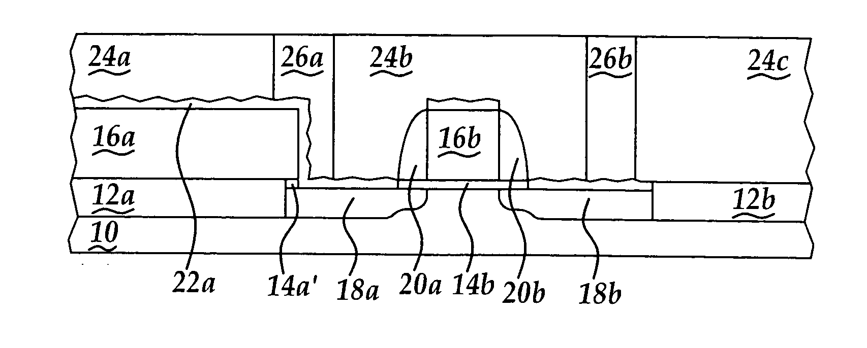
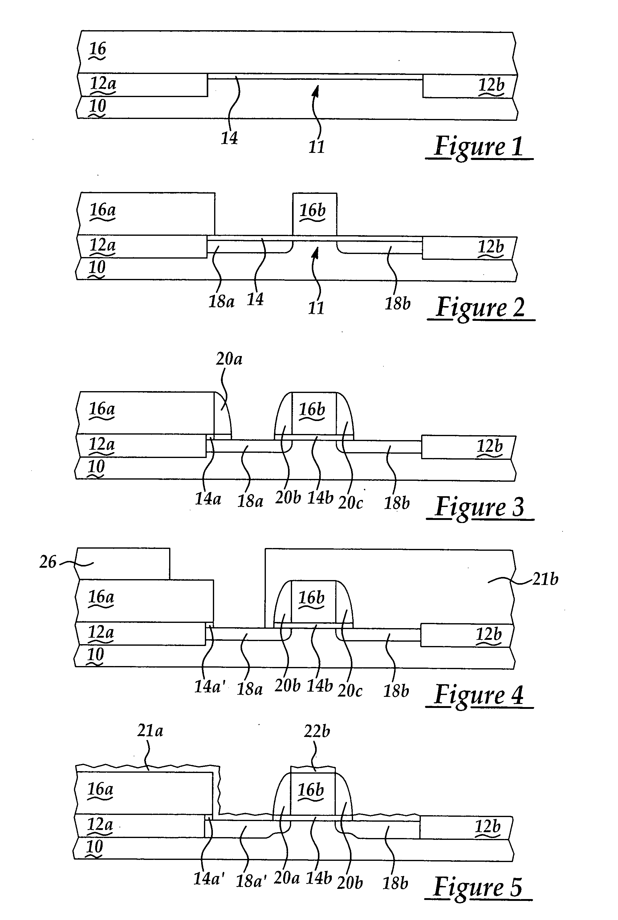
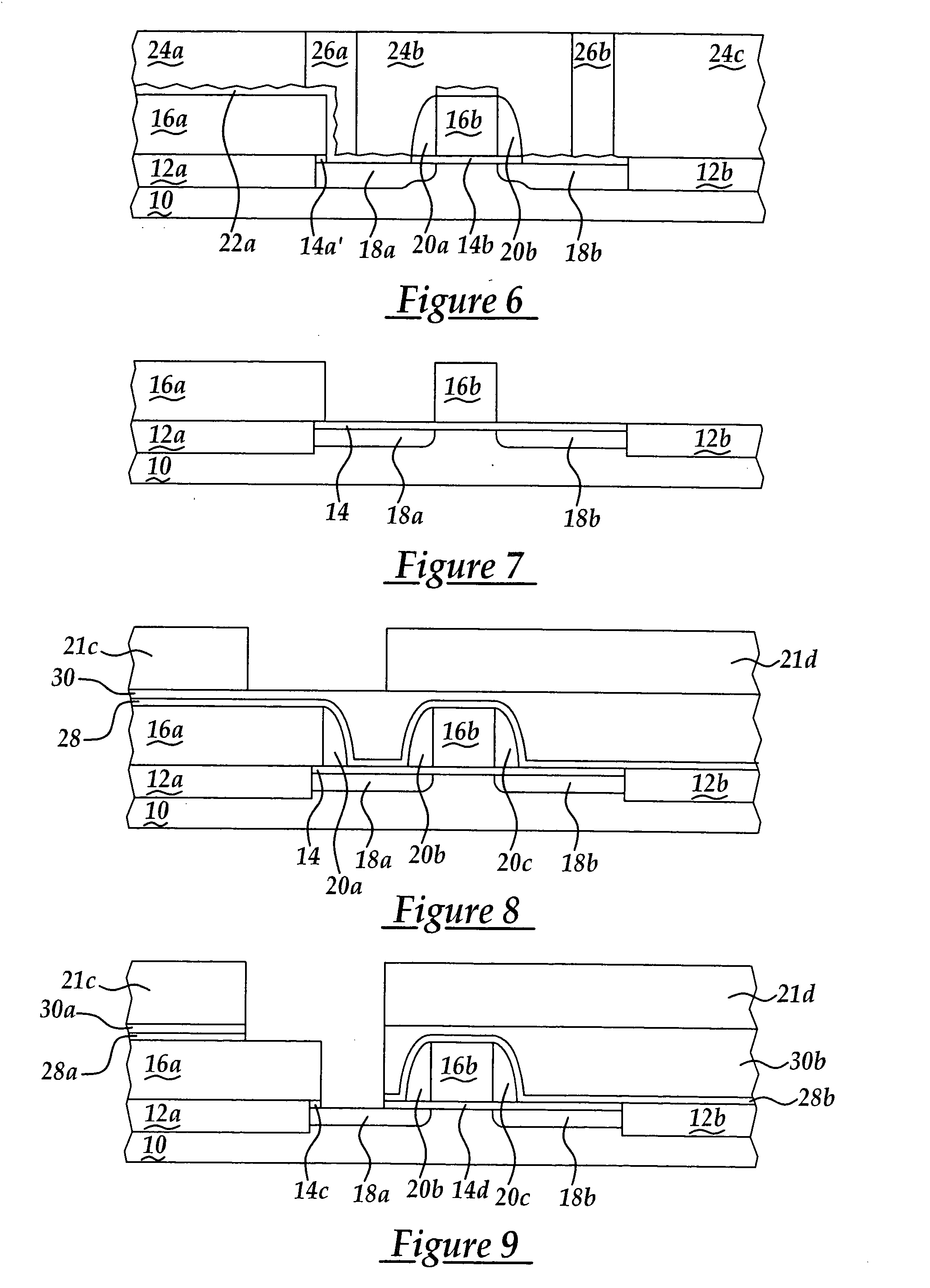
[0015] The invention provides an interconnect structure with enhanced performance, and a method for fabricating the same. The invention realizes the foregoing objects by employing a bridging conductor layer formed upon a contact region within a semiconductor substrate and bridging to a sidewall and a top surface of an interconnect patterned over the contact region of the semiconductor substrate. In particular, by bridging to the top surface of the interconnect, the bridging conductor layer provides an efficient and effective connection between the active region and the interconnect.

[0016]FIG. 1 to FIG. 6 show a series of schematic cross-sectional diagrams illustrating the results of progressive stages in fabricating a semiconductor product in accord with a first preferred embodiment of the invention. FIG. 1 shows a schematic cross-sectional diagram illustrating an early stage in fabricating the semiconductor product.

[0017]FIG. 1 shows a semiconductor substrate 10. A pair of isolat...


PUM


Abstract

An interconnect structure and its method for fabrication each employ an interconnect formed over and adjacent an active region of a semiconductor substrate. A gate electrode is also formed over the active region. Spacer layers are formed adjoining the interconnect and the gate electrode. A spacer layer adjoining the interconnect is removed and a bridging silicide conductor layer is formed bridging a top surface and a sidewall surface of the interconnect with a surface of the active region.

Description

BACKGROUND OF THE INVENTION [0001] 1. Field of the Invention [0002] The invention relates generally to methods for forming interconnect structures within semiconductor products. More particularly, the invention relates to methods for forming interconnect structures with enhanced performance within semiconductor products. [0003] 2. Description of the Related Art [0004] Semiconductor products employ devices such as resistors, transistors, diodes and capacitors that are connected and interconnected over semiconductor substrates. As semiconductor product integration levels increase, effective interconnection of devices often becomes difficult due to lithographic resolution and overlay considerations when forming patterned conductor layers. [0005] Thus, a need exists for semiconductor device interconnect structures and methods with enhanced performance. The invention is directed towards that object. SUMMARY OF THE INVENTION [0006] A first object of the invention is to provide an intercon...

Claims


Application Information

Patent Timeline
Patent Type & Authority Applications(United States)
IPC IPC(8): H01L23/52H01L21/4763
CPCH01L21/76895H01L27/0207H01L27/1104H10B10/12
Inventor LIAW, JHON JHY
Owner TAIWAN SEMICON MFG CO LTD
Why Eureka
Try Eureka