Manufacturing method of solid-state image sensing device

a solid-state image and manufacturing method technology, applied in the direction of radio frequency controlled devices, instruments, television systems, etc., can solve the problems of reducing the mounting area of electronic components, affecting the image display, and causing the failure of connection of bonding wires, so as to improve the manufacturing yield and improve the effect of solid-state image sensing devices

Inactive Publication Date: 2006-05-04
RENESAS TECH CORP +1
View PDF9 Cites 63 Cited by
  • Summary
  • Abstract
  • Description
  • Claims
  • Application Information

AI Technical Summary

Benefits of technology

[0022] Moreover, the manufacturing yield of a solid-state image sensing device can be improved by connecting bonding wires for electrically connecting the electrodes of the main surface of the wiring substrate mounting image sensing elements and the electrodes of the image sensing elements to the bumps formed on the electrodes of the main surface of the wiring substrate.
[0023] In addition, the manufacturing yield of a solid-state image sensing device can be improved by allocating a filter provided between image sensing elements and a lens to the position nearer to the lens than the image sensing elements.
[0024] Further, the manufacturing yield of a solid-state image sensing device can be improved by assembling the system components mounting surface of the wiring substrate and then assembling the optical components mounting surface of the

Problems solved by technology

If foreign matters are deposited to these components, a failure may occur in the image displayed through the solid-stage image sensing device.
However, when sizes are reduced, electronic components mount

Method used


Image

  • Manufacturing method of solid-state image sensing device
  • Manufacturing method of solid-state image sensing device
  • Manufacturing method of solid-state image sensing device

Examples


Embodiment Construction

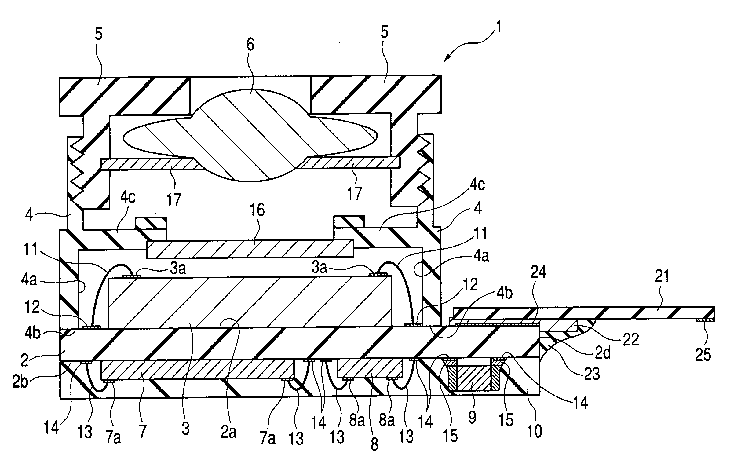
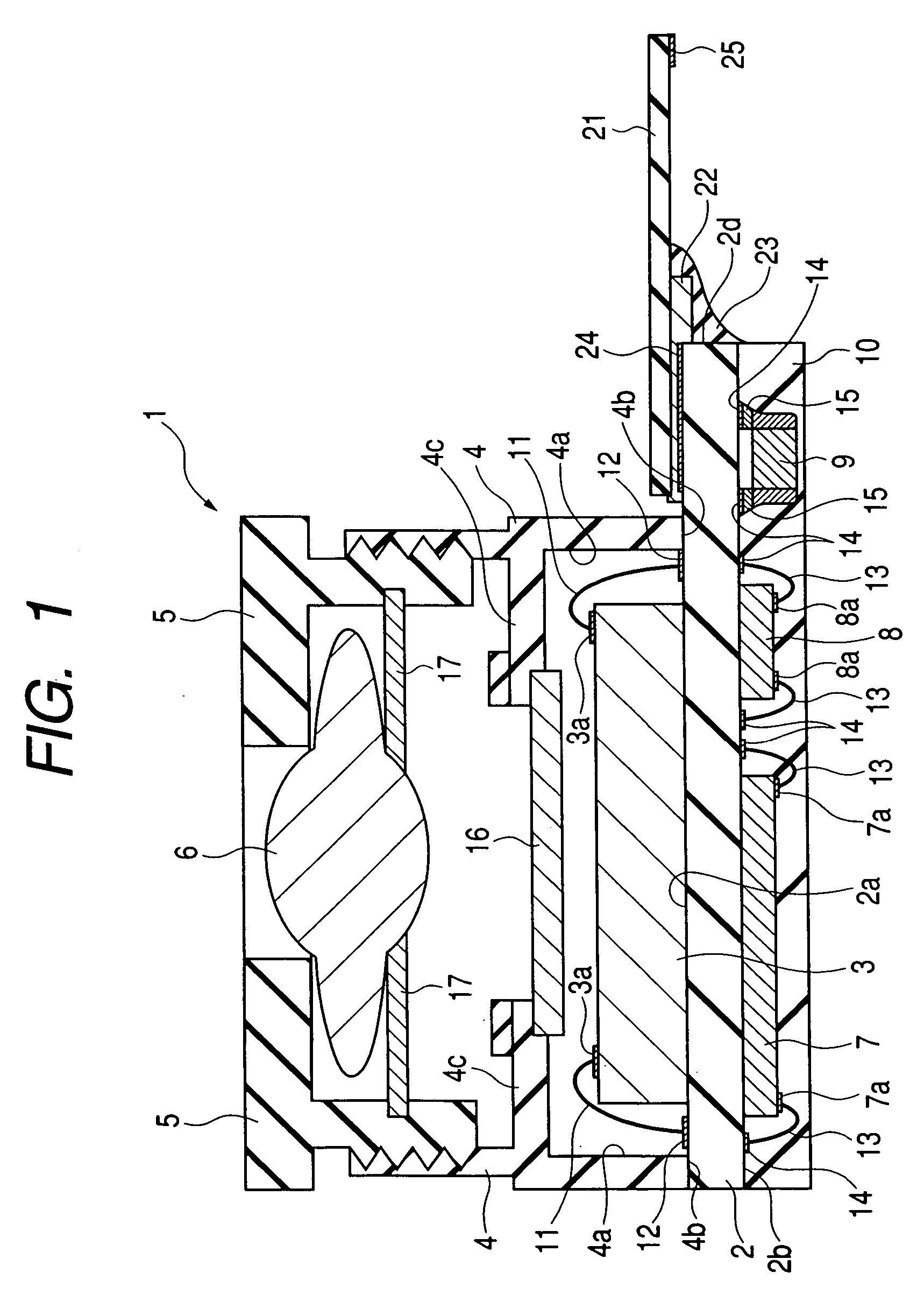
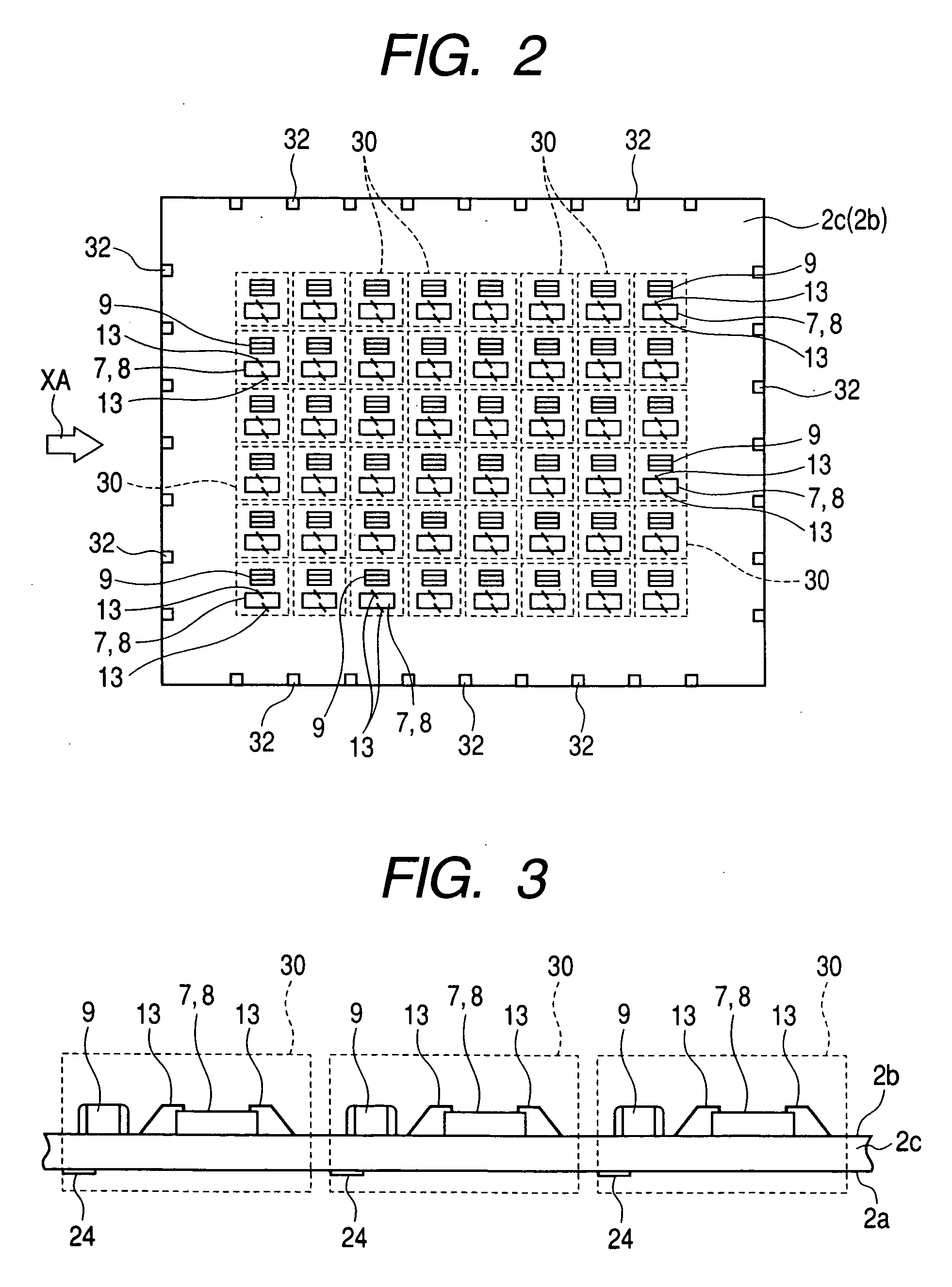
[0062] The preferred embodiment of the present invention will be described in detail with reference to the accompanying drawings. The identical components having the identical functions are indicated by the identical numerals throughout the drawings and the redundant description is avoided. In the following description, the same or similar portions are never described repeatedly, unless otherwise required particularly.

[0063] Moreover, the drawings used for describing the preferred embodiments may include the hatched areas, even if these are plan views, in order to realize easier reading thereof.

[0064] A solid-state image sensing device and a method of manufacturing the same of the present invention will be described with reference to the accompanying drawings. The solid-state image sensing device of the present invention relates to a camera module which is used as an image input portion, for example, of a mobile telephone, a TV phone, a PC camera, a PDA (Personal Digital Assistant...


PUM


Abstract

A sensor chip and a lens mount accommodating therein the sensor chip are mounted on a surface of a wiring substrate and a lens holder accommodating a lens therein is coupled with the lens mount. On a rear surface of the wiring substrate, a logic chip, a memory chip and a passive component are mounted and they are sealed with a seal resin. An electrode pad of the sensor chip is electrically connected to an electrode on the surface of the wiring substrate via a bonding wire but a stud bump is also formed on the electrode at the surface of the wiring substrate and this stud bump is connected with the bonding wire. On the surface of the wiring substrate, a flexible substrate is bonded with an anisotropic conductive film and a bonding material. When a camera module is to be manufactured, the surface side of the wiring substrate is assembled after the rear surface side of the wiring substrate is assembled.

Description

CROSS-REFERENCE TO RELATED APPLICATION [0001] This application is a Continuation of U.S. patent application Ser. No. 10 / 651,087 filed on Aug. 29, 2003, which claims priority from Japanese Patent Application No. 2003-300358, filed on Aug. 25, 2003, the entire disclosure of which is incorporated herein by reference.TECHNICAL FIELD OF THE INVENTION [0002] The present invention relates to a manufacturing method of solid-state image sensing device and particularly to a solid-state image sensing device to be used for a mobile communication device such as a mobile telephone and the technology which can be applied effectively to the same manufacturing method. BACKGROUND OF THE INVENTION [0003] A solid-state image sensing device is a photo-electric converting device for converting an optical signal from an image to an electrical signal by utilizing arrangement of pixels. On the main surface of a substrate of the solid-state image sensing device, image sensing elements are mounted in the cond...

Claims


Application Information

Patent Timeline
IPC IPC(8): H01L31/0232H01L31/062H01L33/00G03B17/02G02B7/02H01L21/60H01L27/14H01L27/146H01L31/0203H04N5/225H04N5/335
CPCH01L24/03H01L2224/0401H01L24/45H01L24/48H01L24/81H01L24/85H01L24/97H01L27/14618H01L27/14683H01L31/0203H01L31/0232H01L2224/05599H01L2224/13144H01L2224/45144H01L2224/48091H01L2224/48095H01L2224/48227H01L2224/48465H01L2224/48475H01L2224/4848H01L2224/48599H01L2224/81801H01L2224/82H01L2224/85051H01L2224/85181H01L2224/86H01L2224/97H01L2924/01004H01L2924/01005H01L2924/01006H01L2924/01029H01L2924/01033H01L2924/01077H01L2924/01078H01L2924/01079H01L2924/01082H01L2924/014H01L2924/19041H01L2924/30105H01L2924/3025H04N5/2253H04N5/2254H04N5/2257H01L2924/00014H01L2924/19105H01L2224/04042H01L24/05H01L2924/181H01L2224/85203H01L2224/85205H01L2924/12043H01L31/02325H01L2224/85444H01L2224/85447H04N23/57H04N23/55H04N23/54H01L2224/85H01L2224/78H01L2924/00H01L2924/00012
Inventor HANADA, KENJINAKANISHI, MASAKIMATSUZAWA, TOMOOSHIDA, KOJITAKASHIMA, KAZUTOSHI
Owner RENESAS TECH CORP
Why Eureka
Try Eureka