

Solid-state image pickup device and driving method therefor
- Summary
- Abstract
- Description
- Claims
- Application Information
AI Technical Summary
Benefits of technology
Problems solved by technology
Method used
Image

Examples
first embodiment
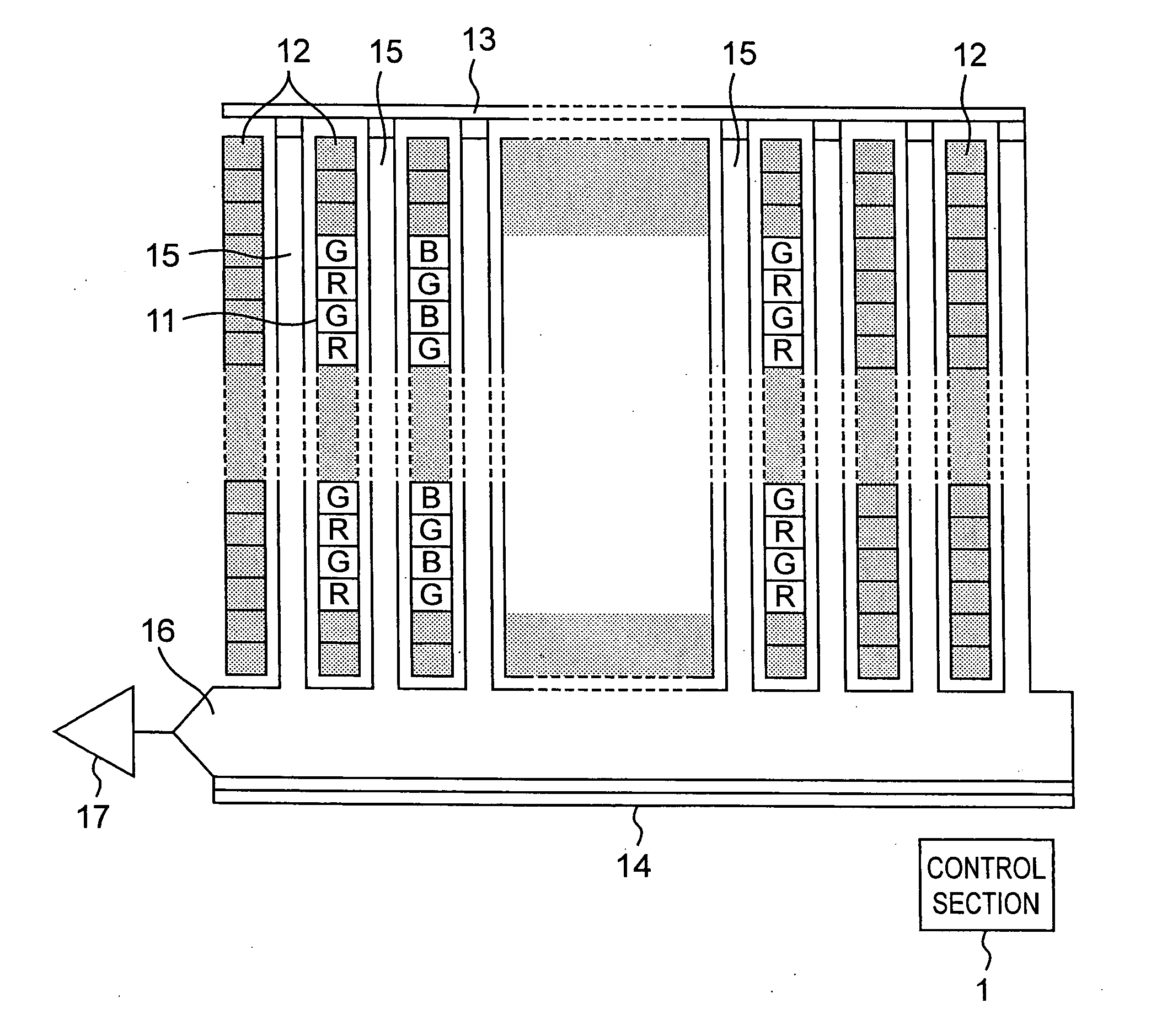
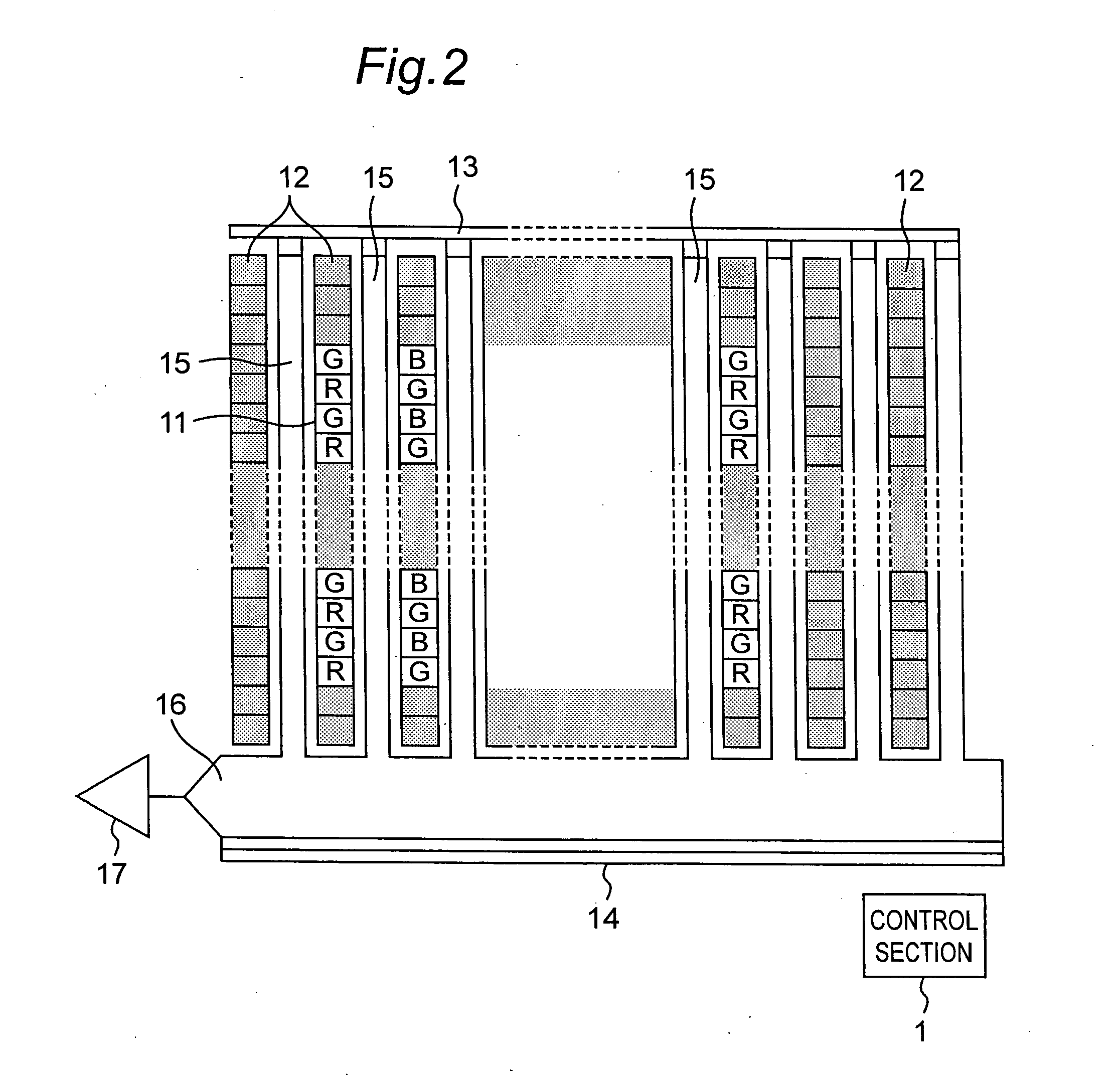
[0065]FIG. 2 is a schematic diagram showing the solid-state image pickup device of the first embodiment of the present invention. The solid-state image pickup device comprises photodiodes 11 which are disposed as light-receiving pixels in the form of a matrix and convert incident light into signal charges, a VCCD 15 which reads signal charges stored in the photodiodes 11 and transfers them in the column direction (vertical direction) as a vertical-transfer section, a HCCD 16 which transfers signal charges from the VCCD 15 in the row direction (horizontal direction) as a horizontal-transfer section, and an output amplifier 17 for amplifying signal charges transferred from the HCCD 16 to output them. The VCCD 15 is provided with a plurality of transfer gates for transferring charges read from the photodiodes 11 in the column direction. Red (R), green (G), and blue (B) color filters are arranged on the photodiodes 11. Furthermore, optical black level regions 12 for generating reference...
second embodiment
[0071]FIG. 8 is a schematic diagram showing the control section 1 provided in the solid-state image pickup device of the second embodiment of the present invention. The control section 1 is the same as for the first embodiment except for the timing pulse producing circuit 27 and timing pulse output section 28 of the timing pulse producing section. In the second embodiment, the same reference numbers are attached to the components having the same functions as those of the first embodiment, and the detail explanation will be omitted.
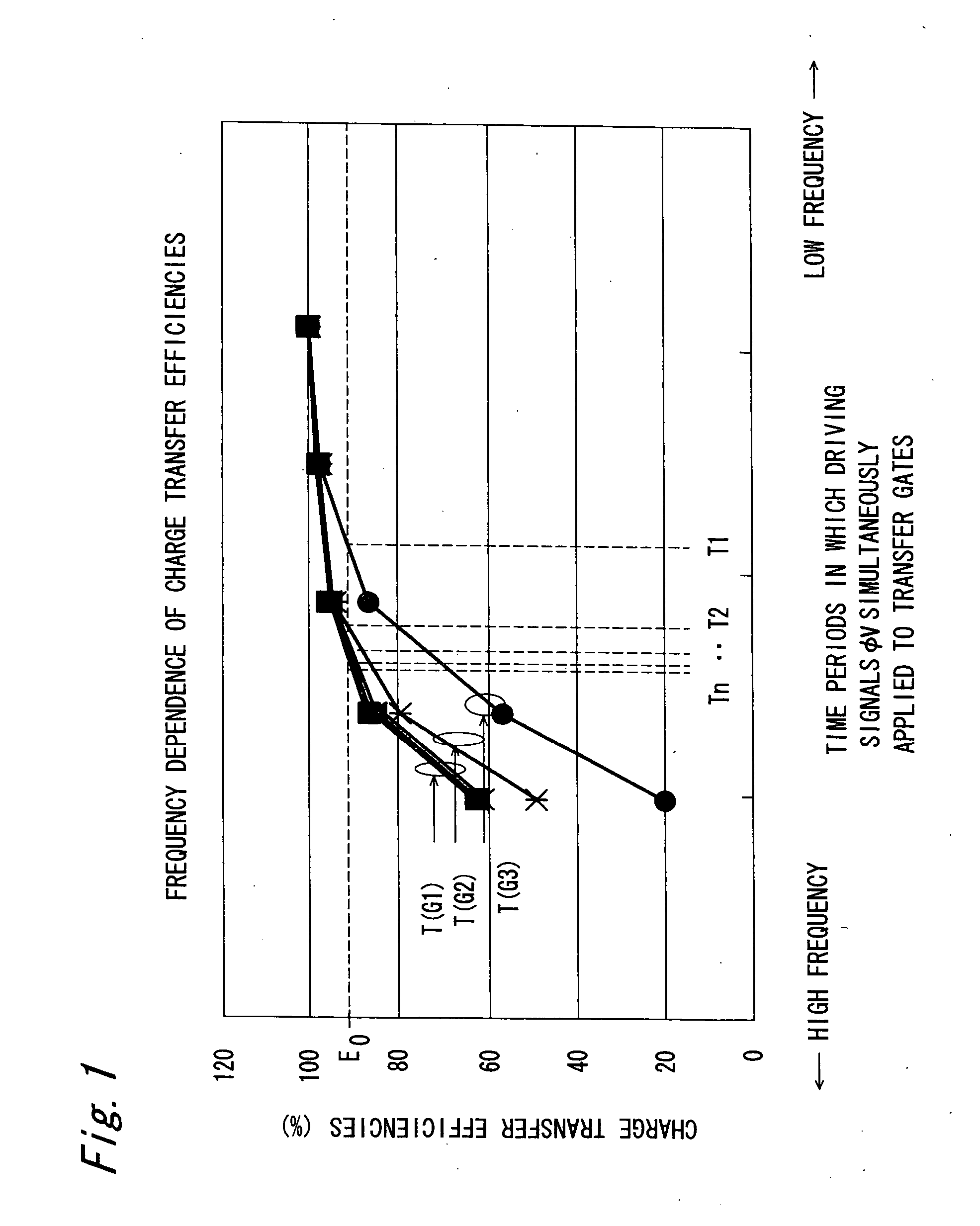
[0072] The timing pulse producing circuit 27 of the control section 1 of this embodiment divides all of the switching periods t1 to tn constituting one cycle of the driving of the VCCD into m groups G1 to Gm less than the number n of the switching periods, and assigns a value of switching period obtained from the frequency dependence of charge transfer efficiencies to each of the groups G1 to Gm.
[0073] Specifically, switching periods t1 to t4 are grouped...
PUM
 Abstract
Description
Claims
Application Information