Liquid crystal display device

Inactive Publication Date: 2006-05-04
PANASONIC LIQUID CRYSTAL DISPLAY CO LTD +1
View PDF13 Cites 93 Cited by
  • Summary
  • Abstract
  • Description
  • Claims
  • Application Information

AI Technical Summary

Benefits of technology

[0014] Further, it is another advantage of the present invention to provide a liquid crystal display device which can reduce a parasitic capacitance.
[0015] Still further, it is another advantage of the present invention to provide a liquid crystal display device which can suppress the difference in image quality attributed to the difference in optical path length in the inside of liquid crystal.
[0016] To briefly explain the summary of typical inventions among inventions disclosed in this specification, they are as follows.
[0017]

Problems solved by technology

That is, depending on the constitution, there may aris

Method used


Image

  • Liquid crystal display device
  • Liquid crystal display device
  • Liquid crystal display device

Examples


Example

Embodiment 1

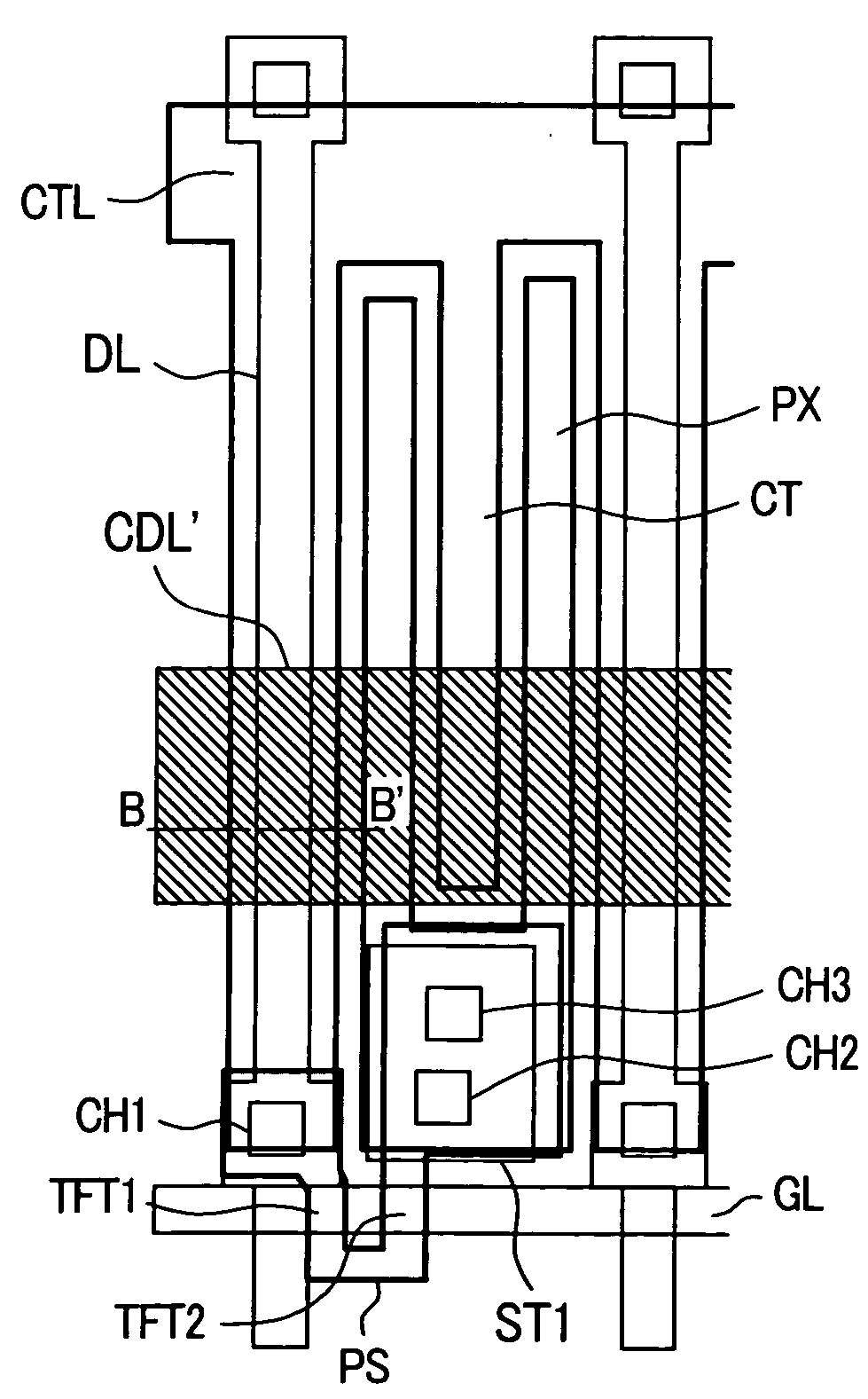
[0104]FIG. 5 is a graph showing one embodiment of an equivalent circuit showing one pixel of the liquid crystal display device according to the present invention, wherein a common signal line CTL runs at a portion corresponding to an upper side of a region of the pixel formed in a rectangular shape, a gate signal line (scanning signal line) GL runs at a portion corresponding to a lower side of the region of the pixel, and a drain signal line (video signal line) DL runs at a portion corresponding to a left side.

[0105] Other pixels which are arranged close to the pixel in the left, right, upper and lower directions have the substantially same constitution, wherein the common signal line CTL and the gate signal line GL are used in common with respect to other pixels which are arranged close to the pixel in the lateral direction, and the drain signal line DL is used in common with respect to other pixels which are arranged close to the pixel in the vertical direction.

[010...

Example

Embodiment 2

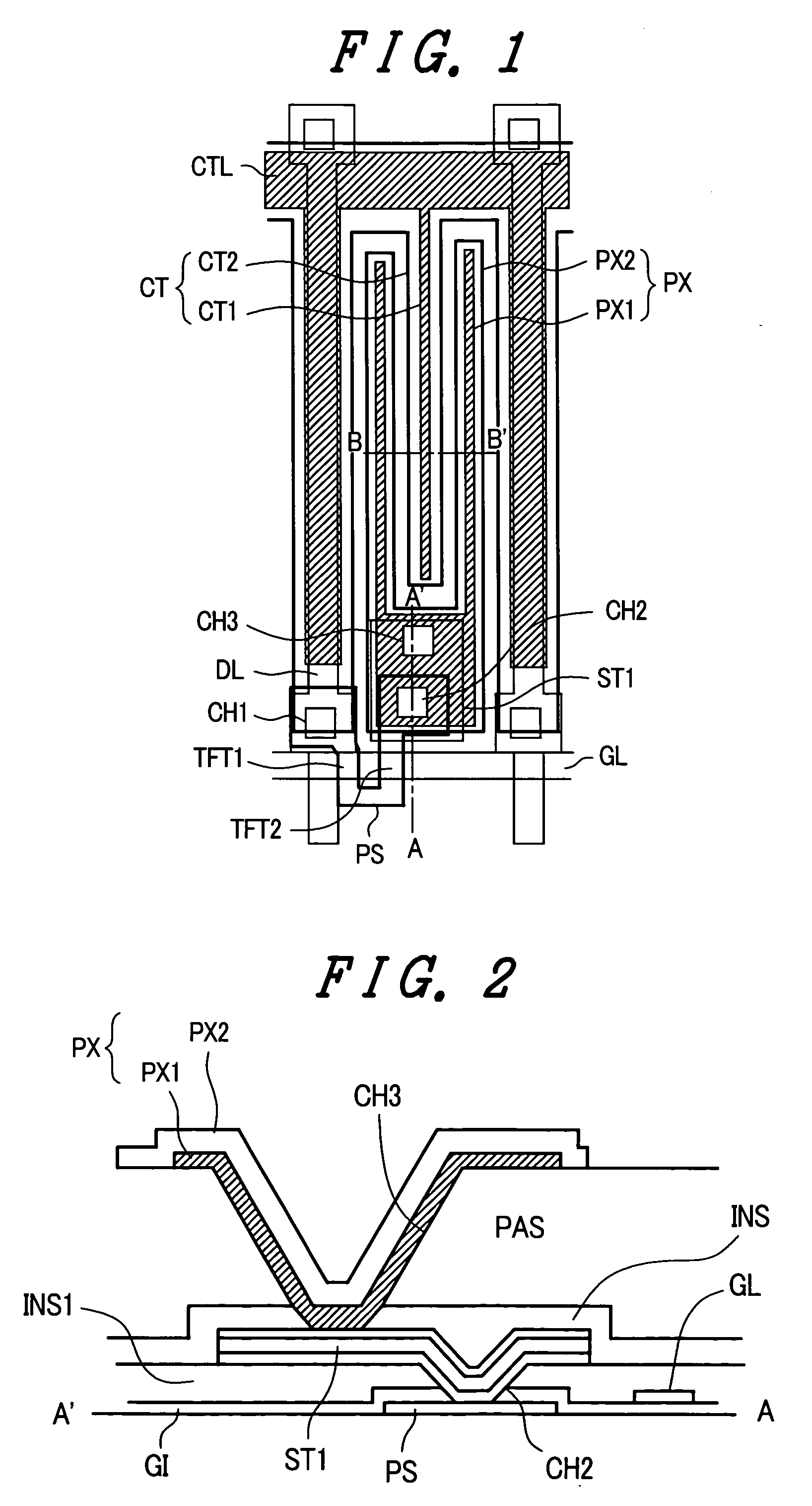
[0158]FIG. 6 is a plan view showing another embodiment of the liquid crystal display device according to the present invention and corresponds to FIG. 1. The liquid crystal display device has an equivalent circuit substantially equal to the equivalent circuit shown in FIG. 5. Further, FIG. 7 is a cross-sectional view taken along a line A-A′ in FIG. 6.

[0159] The constitution which makes this embodiment different from the embodiment shown in FIG. 1 lies, first of all, in that the above-mentioned first metal layers (CT1, PX1) in the counter electrode CT and the pixel electrode PX are formed of the two-layered structure in which, for example, a MoW layer (indicated by symbol PX11 in the drawing) and an Al layer (indicated by symbol PX12 in the drawing) are sequentially stacked.

[0160] Al exhibits the high reflectance (approximately 95%) and hence, it is desirable to adopt the region formed of the Al layer as the reflection region RT.

[0161] Accordingly, for example, the pi...

Example

Embodiment 3

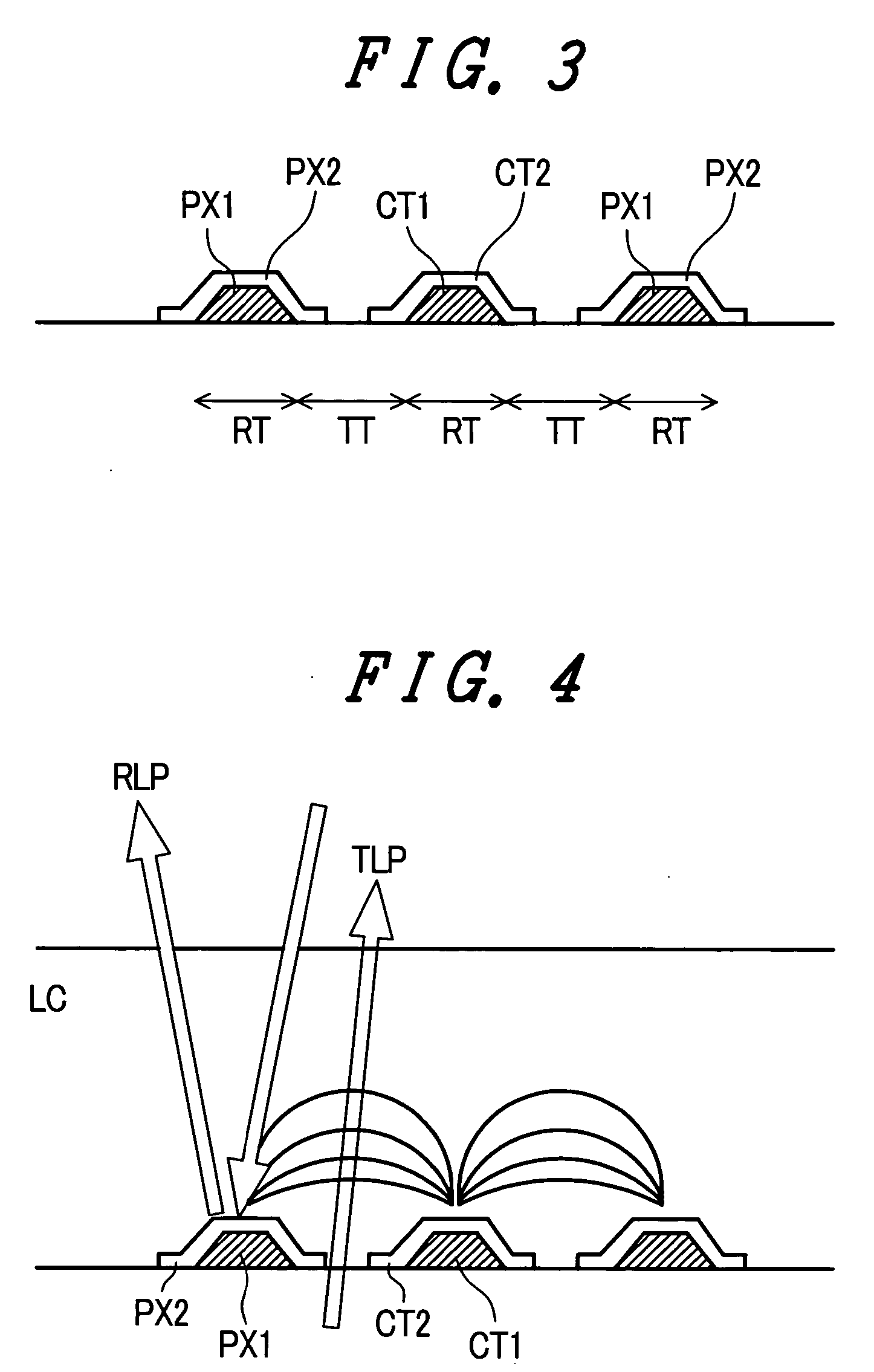
[0166] In the above-mentioned embodiments, the portion which functions as the pixel electrode PX and the counter electrode CT is provided with the pixel electrode PX1 and the counter electrode CT1 which are formed of the reflecting conductive layer. In other words, in the inside of the substantial pixel region (for example, in an aperture region of a black matrix), the transmission region and the reflection region are substantially uniformly arranged.

[0167] However, when it is necessary to allow the transmission region to ensure an area sufficiently larger than an area of the reflection region, it is needless to say that the pixel region is imaginarily divided and one half is configured to possess both of the reflection region RT and the transmission region TT and another half does not possess the reflection region RT and possesses only the transmission region TT.

[0168]FIG. 15 is a plan view of the pixel electrode having such a constitution and corresponds to FIG. 1. ...


PUM


Abstract

The present invention provides a liquid crystal display device which can reduce the difference in brightness between an image obtained from a reflection region and an image obtained from a transmission region. The liquid crystal display device includes a pixel electrode and a counter electrode in each pixel region on a liquid-crystal-side surface of one substrate out of respective substrates which are arranged to face each other with liquid crystal therebetween. The pixel region includes a transmission region and a reflection region. A gap between the pixel electrode and the counter electrode in the reflection region is set larger than the gap between the pixel electrode and the counter electrode in the transmission region.

Description

[0001] The present application claims priority from Japanese application JP2004-316250 filed on Oct. 29, 2004, the content of which is hereby incorporated by reference into this application. BACKGROUND OF THE INVENTION [0002] The present invention relates to a liquid crystal display device, and more particularly to a liquid crystal display device having pixel electrodes and counter electrodes in a pixel region formed on a liquid-crystal-side surface of one substrate out of respective substrates which are arranged to face each other in an opposed manner with liquid crystal therebetween. [0003] This kind of liquid crystal display device is referred to as a so-called lateral electric field type (IPS type) liquid crystal display device, for example, and is known as a display device which has a so-called wide viewing angle characteristic compared to liquid crystal display devices adopting other methods. [0004] On the other hand, although the liquid crystal display device is usually provi...

Claims


Application Information

Patent Timeline
IPC IPC(8): G02F1/1343
CPCG02F1/133555G02F1/134363G02F1/1343
Inventor HASEGAWA, ATSUSHIMIYAZAWA, TOSHIO
Owner PANASONIC LIQUID CRYSTAL DISPLAY CO LTD
Why Eureka
Try Eureka