Fabricating method of semiconductor optical device for flip-chip bonding

Inactive Publication Date: 2006-05-04
SAMSUNG ELECTRONICS CO LTD
View PDF13 Cites 0 Cited by
  • Summary
  • Abstract
  • Description
  • Claims
  • Application Information

AI Technical Summary

Benefits of technology

[0016] Accordingly, the present invention has been made to solve the above-mentioned problems occurring in the prior art and provides additional advantages, by prov

Problems solved by technology

The active alignment method delivers a precise optical axis alignment, but requires a relatively longer processing time, which is not suitable for the mass-production thereof.
Accordingly, when forming the

Method used


Image

  • Fabricating method of semiconductor optical device for flip-chip bonding
  • Fabricating method of semiconductor optical device for flip-chip bonding
  • Fabricating method of semiconductor optical device for flip-chip bonding

Examples


Embodiment Construction

[0023] Hereinafter, embodiments of the present invention will be described with reference to the accompanying drawings. For the purposes of clarity and simplicity, a detailed description of known functions and configurations incorporated herein will be omitted as it may make the subject matter of the present invention unclear.

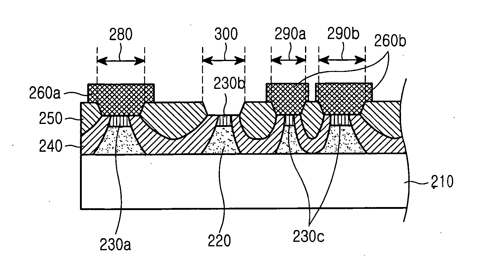
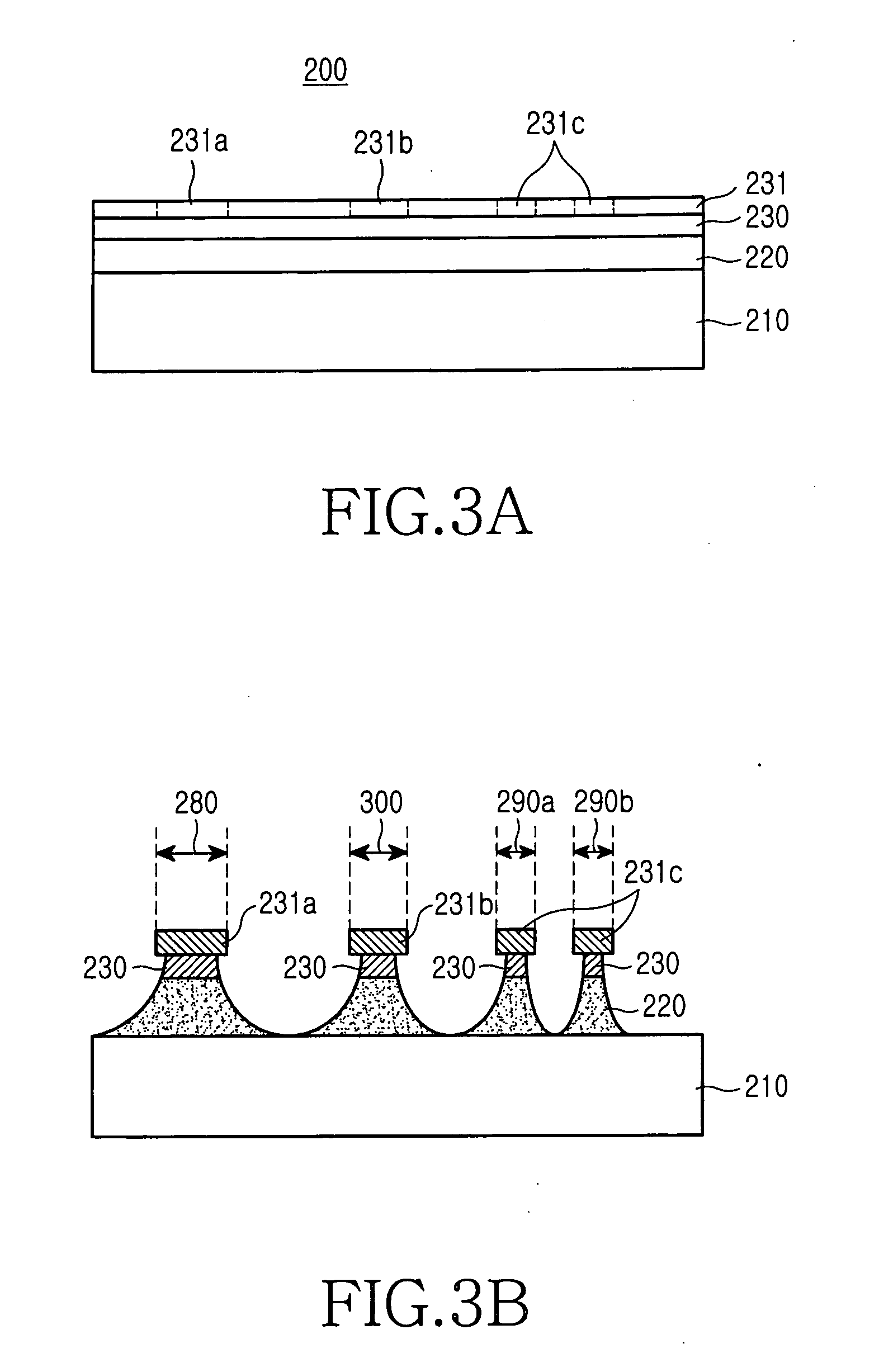
[0024] Referring to FIGS. 3a to 3e, a method of manufacturing a semiconductor optical device for flip-chip bonding according to the present invention briefly includes an etching process in which an active layer 220 and a clad 230 stacked on a semiconductor substrate 210 in sequence are etched to form a mesa structure, a growing process in which current insulating layers 240 and 250 are grown at a mesa-etched portion between the active layer 220 and the clad 230, and an electrode forming process of forming an electrode 270.

[0025] The etching process comprises a growing step and an etching step, mesa-etching the active layer 220 and the clad 230 according to al...


PUM


Abstract

Disclosed is a method for manufacturing a semiconductor optical device for flip-chip bonding. The method includes the steps of: etching an active layer and clad which are sequentially stacked on a semiconductor substrate into first and second alignment keys and an optical area, which has a mesa structure; growing at least two insulating layers at mesa-etched portions between the first and second alignment keys and the optical areas; and forming protection masks on the first and second alignment keys, growing an electrode on the optical area and the insulating layer except for the protection masks, and removing the protection masks.

Description

CLAIM OF PRIORITY [0001] This application claims priority to an application entitled “Fabricating method of semiconductor optical device for flip-chip bonding,” filed in the Korean Intellectual Property Office on Nov. 3, 2004 and assigned Serial No. 2004-89031, the contents of which are hereby incorporated by reference. BACKGROUND OF THE INVENTION [0002] 1. Field of the Invention [0003] The present invention relates to a method for manufacturing a semiconductor and, more particularly, to a method of manufacturing a semiconductor optical device having at least one optical axis alignment key. [0004] 2. Description of the Related Art [0005] Semiconductor optical devices include a light source for generating light and a light-receiving device for receiving the light. A semiconductor laser is typically used as the semiconductor light source and includes an optical device that is aligned with a planar lightwave circuit (PLC). A passive alignment method and an active alignment method are m...

Claims


Application Information

Patent Timeline
IPC IPC(8): H01L21/00
CPCH01S5/0224H01S5/227H01S5/0234Y10S438/975H01L31/00
Inventor KIM, YOUNG-HYUNKIM, INBAE, YU-DONGBANG, YOUNG-CHURL
Owner SAMSUNG ELECTRONICS CO LTD
Why Eureka
Try Eureka