Wafer to wafer bonding apparatus, wafer to wafer bonding system, and wafer to wafer bonding method

a technology of wafers and junction points, applied in the direction of electrical equipment, basic electric elements, semiconductor devices, etc., can solve the problems of bonding errors between junction points of wafers, and achieve the effect of reducing alignment errors

Inactive Publication Date: 2021-05-13
SAMSUNG ELECTRONICS CO LTD
View PDF0 Cites 1 Cited by
  • Summary
  • Abstract
  • Description
  • Claims
  • Application Information

AI Technical Summary

Benefits of technology

[0011]Thus, heat from the heating elements may be transferred to the wafer in contact or non-contact form to thereby minimize the alignment error between the wafers.

Problems solved by technology

Local portions of at least one of the first and second wafers may be deformed due to initial warpage of the wafer, anisotropy of the wafer material, and the like, thereby resulting in bonding errors between junction points in the wafers.

Method used


Image

  • Wafer to wafer bonding apparatus, wafer to wafer bonding system, and wafer to wafer bonding method
  • Wafer to wafer bonding apparatus, wafer to wafer bonding system, and wafer to wafer bonding method
  • Wafer to wafer bonding apparatus, wafer to wafer bonding system, and wafer to wafer bonding method

Examples


Embodiment Construction

[0027]Hereinafter, example embodiments will be explained in detail with reference to the accompanying drawings.

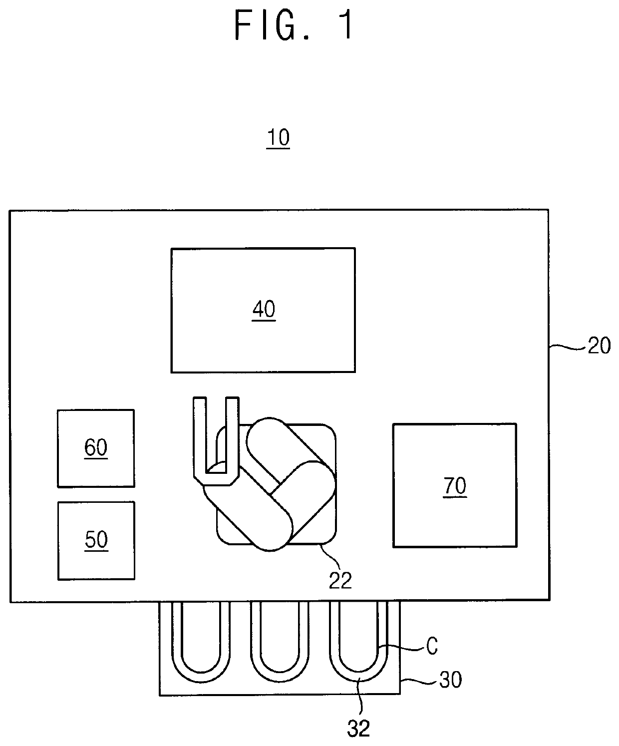
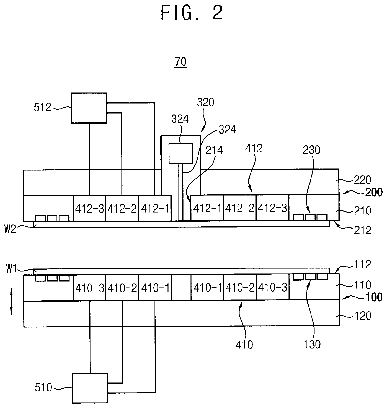
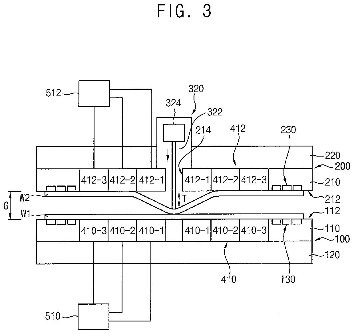
[0028]FIG. 1 is a block diagram illustrating a wafer to wafer bonding system according to exemplary embodiments.

[0029]Referring to FIG. 1, a wafer to wafer bonding system 10 may include a pre-treatment apparatus such as a plasma processing apparatus 40 and a cleaning apparatus 50, an alignment apparatus 60, and a wafer bonding apparatus 70 arranged in a clean room 20. The wafer to wafer bonding system 10 may further include a cassette stage 30 disposed in a side of the clean room 20, for example.

[0030]In example embodiments, the clean room 20 may be an enclosed room having a cuboid shape, and may be a controlled environment that has a low level of pollutants such as, for example, dust, airborne microbes, aerosol particles, and chemical vapors.

[0031]The cassette stage 30 may provide a space in which wafers are located before being transferred into the clean room 20. A carrie...


PUM

PropertyMeasurementUnit
central angleaaaaaaaaaa
wavelengthaaaaaaaaaa
angleaaaaaaaaaa

Abstract

A wafer bonding apparatus includes a lower stage having a first surface and holding a first wafer on the first surface, an upper stage having a second surface and holding a second wafer on the second surface, an upper push rod passing through a center hole of the upper stage to press a middle region of the second wafer, and a plurality of first heating circuits provided at the second surface of the upper stage to heat the second wafer held by the upper stage. Each of the plurality of first heating circuits is independently controlled such that the second wafer is heated to have different temperature distributions along a circumferential direction about a center of the second wafer.

Description

PRIORITY STATEMENT[0001]This application claims priority under 35 U.S.C. § 119 to Korean Patent Application No. 10-2019-0143486, filed on Nov. 11, 2019 in the Korean Intellectual Property Office (KIPO), the contents of which are herein incorporated by reference in their entirety.BACKGROUND1. Field[0002]Example embodiments relate to a wafer bonding apparatus, a wafer to wafer bonding system and a wafer to wafer bonding method. More particularly, example embodiments relate to an apparatus for boding wafers to each other to manufacture a semiconductor device having a three-dimensional connection structure, a wafer to wafer bonding apparatus and a wafer to wafer bonding method.2. Description of the Related Art[0003]In manufacturing electronic products such as a CIS (CMOS image sensor), an HBM (High Bandwidth Memory), etc., two wafers may be bonded to each other, thereby increasing a production yield per wafer. The wafer to wafer bonding process may include an O2 plasma activation step, ...

Claims


Application Information

Patent Timeline
Patent Type & Authority Applications(United States)
IPC IPC(8): H01L21/67H01L21/683H01L33/00H01L21/68H01L33/48
CPCH01L21/67092H01L21/6838H01L33/486H01L33/0093H01L21/682H01L21/67098H01L21/67103H01L21/67248H01L21/185H01L21/324H01L21/68742H01L24/27H01L24/28H01L24/743H01L24/75H01L24/83H01L33/00
Inventor LIM, KYEONGBINKIM, JUNHYUNGWOO, SIWOONGSEOK, SEUNGDAE
Owner SAMSUNG ELECTRONICS CO LTD
Why Eureka
Try Eureka