Electron emission device, manufacturing method of the device

a technology of electron emission and manufacturing method, which is applied in the manufacture of electrode systems, electric discharge tubes/lamps, and discharge tubes luminescent screens, etc., can solve the problems of unintentional differences in voltage applied to electron emission regions, deterioration of illumination uniformity of pixels, and drop in voltage, so as to enhance the electron emission of each pixel, the effect of increasing the effective width of the cathode electrode and increasing the degree of integration of electron emission regions

Inactive Publication Date: 2008-02-21
SAMSUNG SDI CO LTD
View PDF10 Cites 2 Cited by
  • Summary
  • Abstract
  • Description
  • Claims
  • Application Information

AI Technical Summary

Benefits of technology

[0012]Exemplary embodiments of the present invention provide an electron emission device, in which a degree of integration of electron emission regions is increased while providing resistive layers on cathode electrodes to thereby enhance electron emission of each pixel, and an effective width of the cathode electrodes is increased to prevent a drop in voltage.

Problems solved by technology

During operation of the light emission device, a drop in voltage may occur as a result of an unstable driving voltage being applied to the driving electrodes or due to an internal resistance of the driving electrodes.
This may result in unintentional differences in voltages applied to the electron emission regions.
When this occurs, the emission characteristics of the electron emission regions become uneven, thereby resulting in deterioration in the illumination uniformity of the pixels.
This makes it difficult for a sufficient amount of electrons to be supplied to each of the pixels, thereby resulting in a drop in screen brightness.
Further, as a result of the apertures, the effective width through which current actually flows in the cathode electrodes is reduced thereby, causing a sharp drop in voltage.
However, during manufacture, alignment errors may result among the cathode electrodes, isolation electrodes, and resistive layers.
In this case, contact defects may occur between the resistive layers and the cathode electrodes, as well as between the resistive layers and the isolation electrodes, such that the flow of current to the electron emission regions may be cut off.

Method used


Image

  • Electron emission device, manufacturing method of the device
  • Electron emission device, manufacturing method of the device
  • Electron emission device, manufacturing method of the device

Examples


Embodiment Construction

[0031]In exemplary embodiments of the present invention, “light emission device” refers to all devices that emit visible light. Accordingly, all displays that display symbols, letters, numbers, and images to transmit information are also encompassed within the meaning of the term light emission device as it is used herein. In addition, light emission device may also refer to light sources that provide light to a non-emissive display panel.

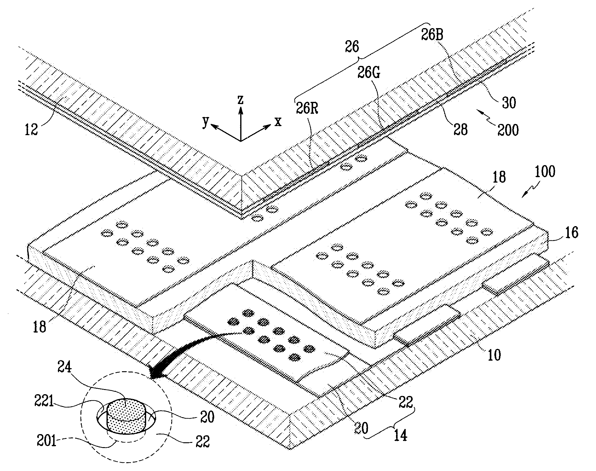
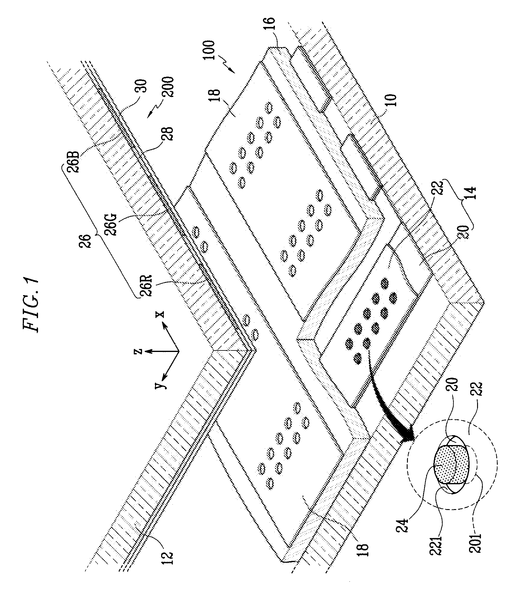
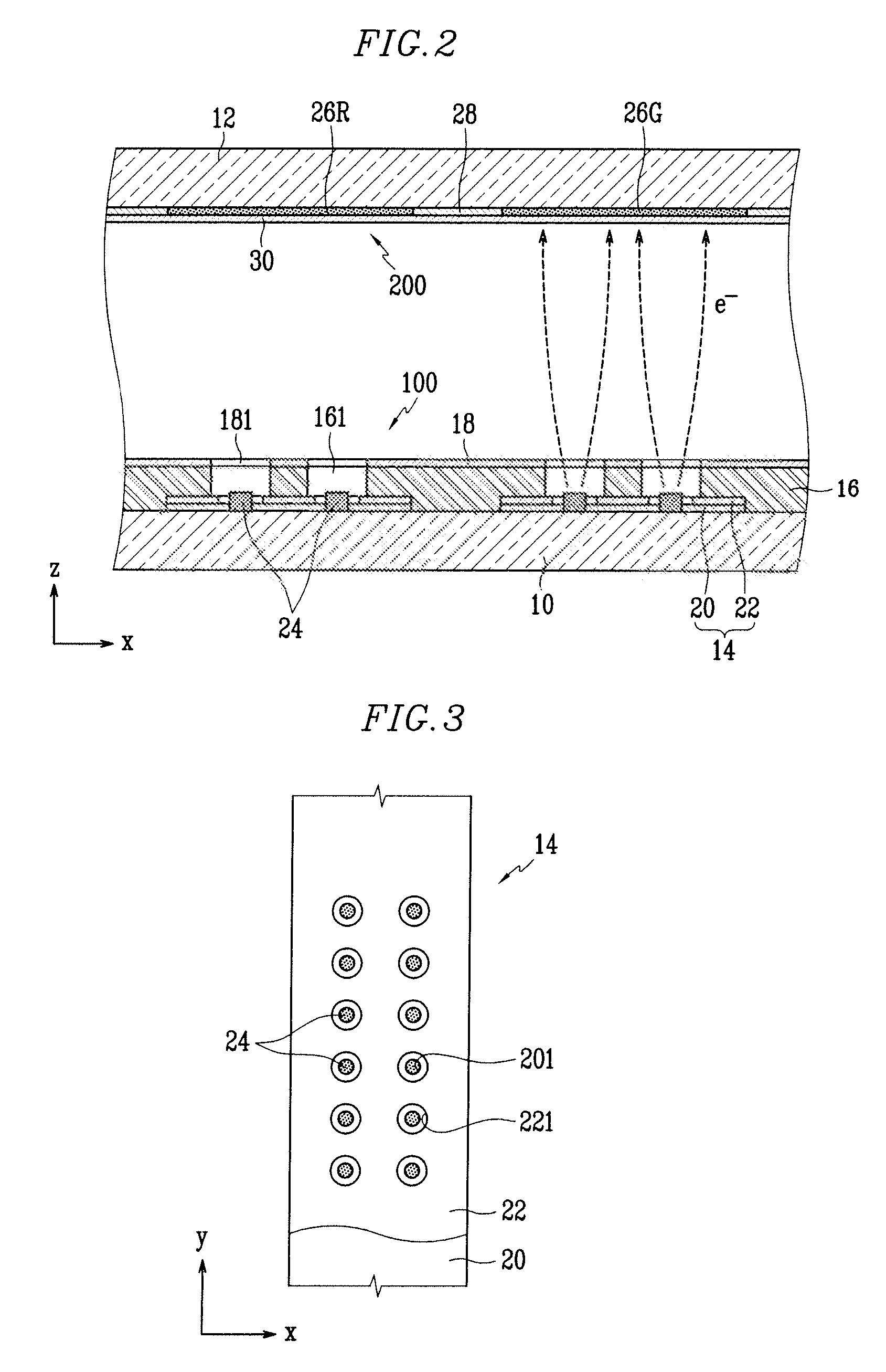
[0032]Referring to FIGS. 1-3, a light emission device according to a first exemplary embodiment of the present invention includes a first substrate 10 and a second substrate 12 facing one another in a substantially parallel manner and with a predetermined gap therebetween. A sealing member (not shown) is provided between the first and second substrates 10, 12 along the edge portions thereof to seal together the first and second substrates 10, 12 and thus form a vacuum vessel. In one embodiment, the interior of the vacuum vessel is kept to a degree ...


PUM


Abstract

An electron emission device includes a substrate, cathode electrodes and gate electrodes formed on the substrate crossing one another to thereby form a plurality of crossed regions, and electron emission regions, each electrically coupled to one of the cathode electrodes. Each of the cathode electrodes includes a resistive layer formed with first openings, and a conductive layer disposed on one surface of the resistive layer, and formed with second openings. The second openings are spatially communicated respectively with the first openings, and circumferential wall portions of the conductive layer defining the second openings maintain a predetermined spacing from circumferential wall portions of the resistive layer defining the first openings. The electron emission regions are then disposed in the first openings.

Description

CROSS-REFERENCE TO RELATED APPLICATION[0001]This application claims priority to and the benefit of Korean Patent Application No. 10-2006-54921 filed on Jun. 19, 2006 in the Korean Intellectual Property Office, the entire content of which is incorporated herein by reference.BACKGROUND OF THE INVENTION[0002]1. Field of the Invention[0003]The present invention relates to an electron emission device having a cathode electrode on which a resistance layer is disposed to increase an electron emission uniformity of the electron emission device. The present invention relates also to a manufacturing method of the electron emission device and to a light emission device using the electron emission device.[0004]2. Description of Related Art[0005]There are many different types of light emission devices that radiate visible light. One type of light emission device includes a structure in which electron emission elements are disposed on a first substrate, and a phosphor layer and an anode electrode...

Claims


Application Information

Patent Timeline
Patent Type & Authority Applications(United States)
IPC IPC(8): H01J63/04
CPCH01J9/025H01J2329/0497H01J63/04H01J31/127
Inventor HAN, SAM-ILAHN, SANG-HYUCKLEE, SANG-JOJEON, SANG-HOCHO, JIN-HUIHONG, SU-BONG
Owner SAMSUNG SDI CO LTD
Why Eureka
Try Eureka