Optical module

a technology of optical modules and optical components, applied in the field of optical modules, can solve the problems of complex structure and increase in the price of parts, and achieve the effects of reducing the error of light alignment, simple process and equipment, and aligning light with small expenses

Inactive Publication Date: 2017-11-28
ELECTRONICS & TELECOMM RES INST
View PDF9 Cites 1 Cited by
  • Summary
  • Abstract
  • Description
  • Claims
  • Application Information

AI Technical Summary

Benefits of technology

[0007]An embodiment of the present invention relates to an optical module capable of minimizing an alignment error, reducing an expense, and simplifying process equipment.
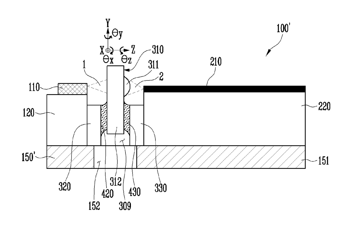
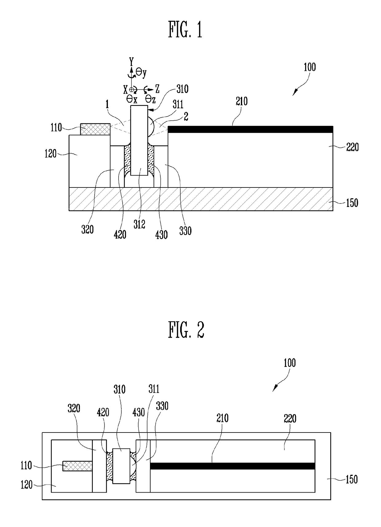
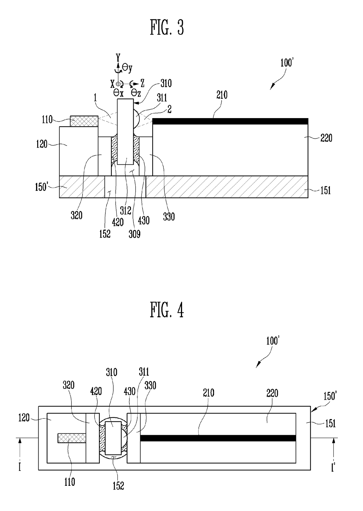
[0024]According to an embodiment of the present invention, since a degree of freedom of light alignment in the optical axis direction is removed by the pair of lens mounts and a contact area between the lens system and the lens mounts increases, it is possible to minimize an error during light alignment and to align light with small expenses and simple processes and equipment.
[0025]Since it is possible to minimize force of static friction and electrostatic force between the lens mount and the lens system by forming the plurality of grooves in the pair of lens mounts, it is possible to easily align light. Since it is possible to minimize gripping force of a gripper, it is possible to prevent the lens system from being damaged by the gripping force.
[0026]Although viscosity of an adhesive is low or a large amount of adhesive is implanted, since it is possible to prevent the adhesive from spreading to a neighboring channel due to the plurality of grooves provided in the pair of lens mounts, it is possible to make the multi-channel optical module small.

Problems solved by technology

The conventional optical module needs a high-temperature heater or a high-output laser for soldering melting, has a complicated structure, and includes parts prices of which increase.

Method used


Image

  • Optical module
  • Optical module
  • Optical module

Examples


Embodiment Construction

[0045]Advantages and features of the present invention, and implementation methods thereof will be clarified through following embodiments described with reference to the accompanying drawings. The present invention may, however, be embodied in different forms and should not be construed as limited to the embodiments set forth herein. Throughout this specification and the claims that follow, when it is described that an element is “connected” to another element, the element may be “directly connected” to the other element or “electrically connected” to the other element through a third element. In the accompanying drawings, a portion irrelevant to description of the present invention will be omitted for clarity. Like reference numerals refer to like elements throughout.

[0046]Hereinafter, embodiments will be described in detail so that those skilled in the art may easily perform the present invention with reference to the accompanying drawings.

[0047]FIG. 1 is a side view of an optica...


PUM


Abstract

There is provided an optical module. The optical module includes a light source, a wave guide to which beam output from the light source is input, a lens system configured to optically combining the light source and the wave guide, a first lens mount positioned between the light source and the lens system in an optical axis of the light source, a first adhesive configured to fix the lens system to the first lens mount, a second lens mount positioned between the wave guide and the lens system in the optical axis of the light source, and a second adhesive configured to fix the lens system to the second lens mount. Therefore, it is possible to precisely align light, to manufacture the optical module with small expenses, and to simplify processes and equipment.

Description

CROSS-REFERENCE TO RELATED APPLICATION[0001]The present application claims priority to Korean Patent Application Number 10-2016-0021811 filed on Feb. 24, 2016, the entire disclosure of which is incorporated herein in its entirety by reference.BACKGROUND[0002]1. Field[0003]An embodiment of the present invention relates to an optical module, and more particularly, to an optical module in which a light source and a wave guide are aligned by a lens.[0004]2. Description of the Related Art[0005]A light source and a wave guide that are provided in an optical module may be optically combined by a lens. At this time, a position of the lens is controlled so that an amount of light incident on the wave guide has a maximum value in order to align light between the light source and the wave guide. In a conventional optical module, in order to fix the lens the position of which is controlled, soldering heating or laser welding is used. The conventional optical module needs a high-temperature heat...

Claims


Application Information

Patent Timeline
Patent Type & Authority Patents(United States)
IPC IPC(8): G02B6/42
CPCG02B6/4244G02B6/4204G02B6/4245G02B6/425G02B6/4239G02B6/424F21K9/20F21K9/60F21S2/005F21V5/007F21Y2115/30F21Y2101/00
Inventor LEE, JONG JINLIM, KWON-SEOBKIM, DAE SEONLEE, SUN-GOO
Owner ELECTRONICS & TELECOMM RES INST
Why Eureka
Try Eureka