Supercharge Your Innovation With Domain-Expert AI Agents!

Method for forming semiconductor device

a silicon-insulator and fet technology, applied in semiconductor devices, semiconductor/solid-state device details, electrical devices, etc., can solve the problems of parasitic bipolar action, high leakage current of floating body soi devices, and disadvantages of conventional soi transistors

Inactive Publication Date: 2006-05-04
LAPIS SEMICON CO LTD
View PDF6 Cites 0 Cited by
  • Summary
  • Abstract
  • Description
  • Claims
  • Application Information

AI Technical Summary

Benefits of technology

The present invention provides a method for making a silicon-on-insulator FET that can have ions implanted to the surface of the substrate via the contact hole for substrate-biasing. This method prevents the contact hole for substrate-biasing from causing an opening fault. The method involves forming a semiconductor substrate with an insulating layer, adding a silicon layer on top, creating a first conductive contact layer that connects to the substrate, adding an interlayer-insulating layer, creating a through-hole in the interlayer-insulating layer that matches the first conductive contact layer, and then adding a second conductive contact layer to fill the through-hole. This method allows for the creation of a reliable and efficient silicon-on-insulator FET.

Problems solved by technology

Floating body SOI devices can experience high leakage current and parasitic bipolar action.
The conventional SOI transistor has a performance disadvantage.

Method used


Image

  • Method for forming semiconductor device
  • Method for forming semiconductor device
  • Method for forming semiconductor device

Examples


Embodiment Construction

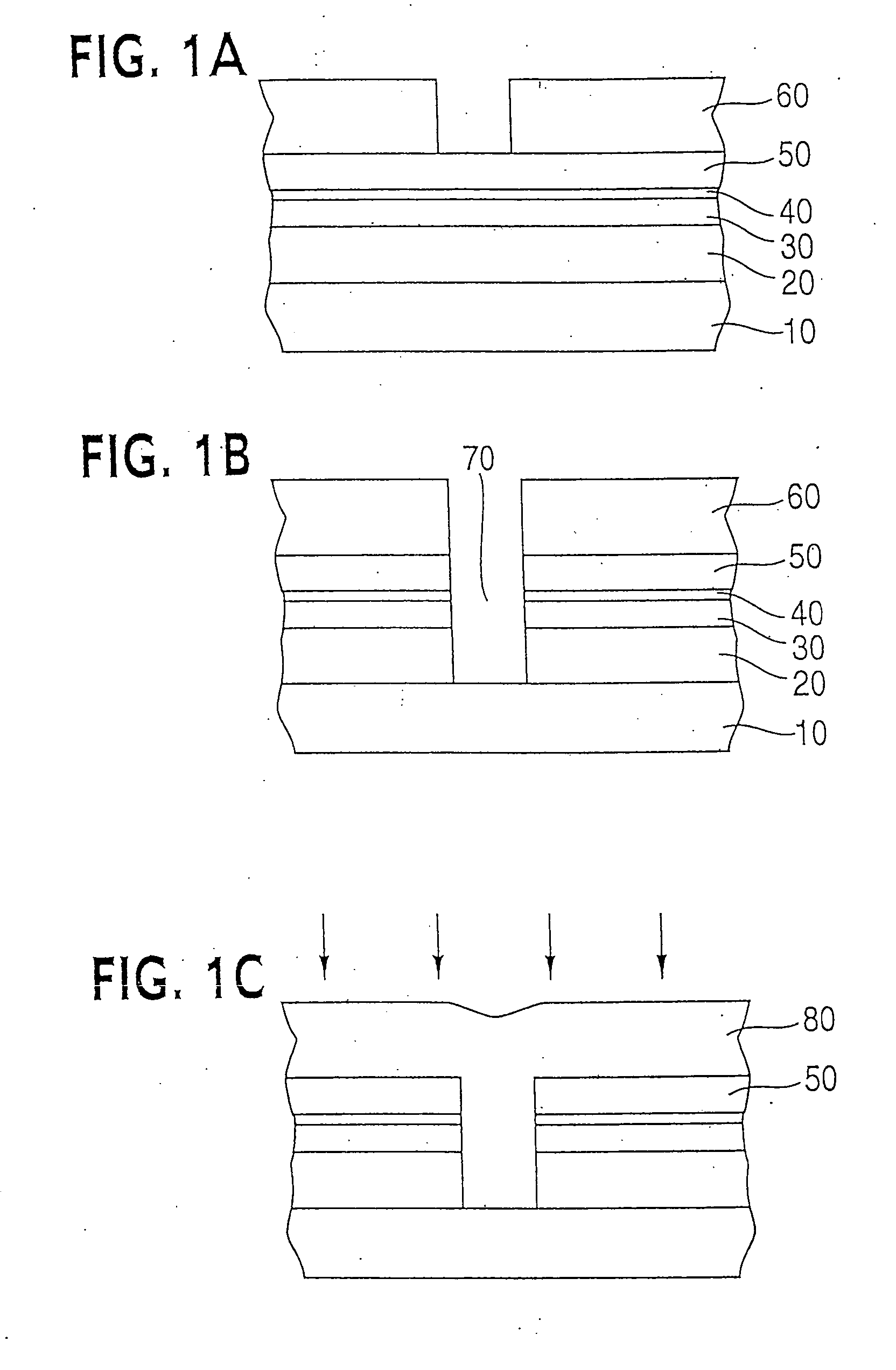
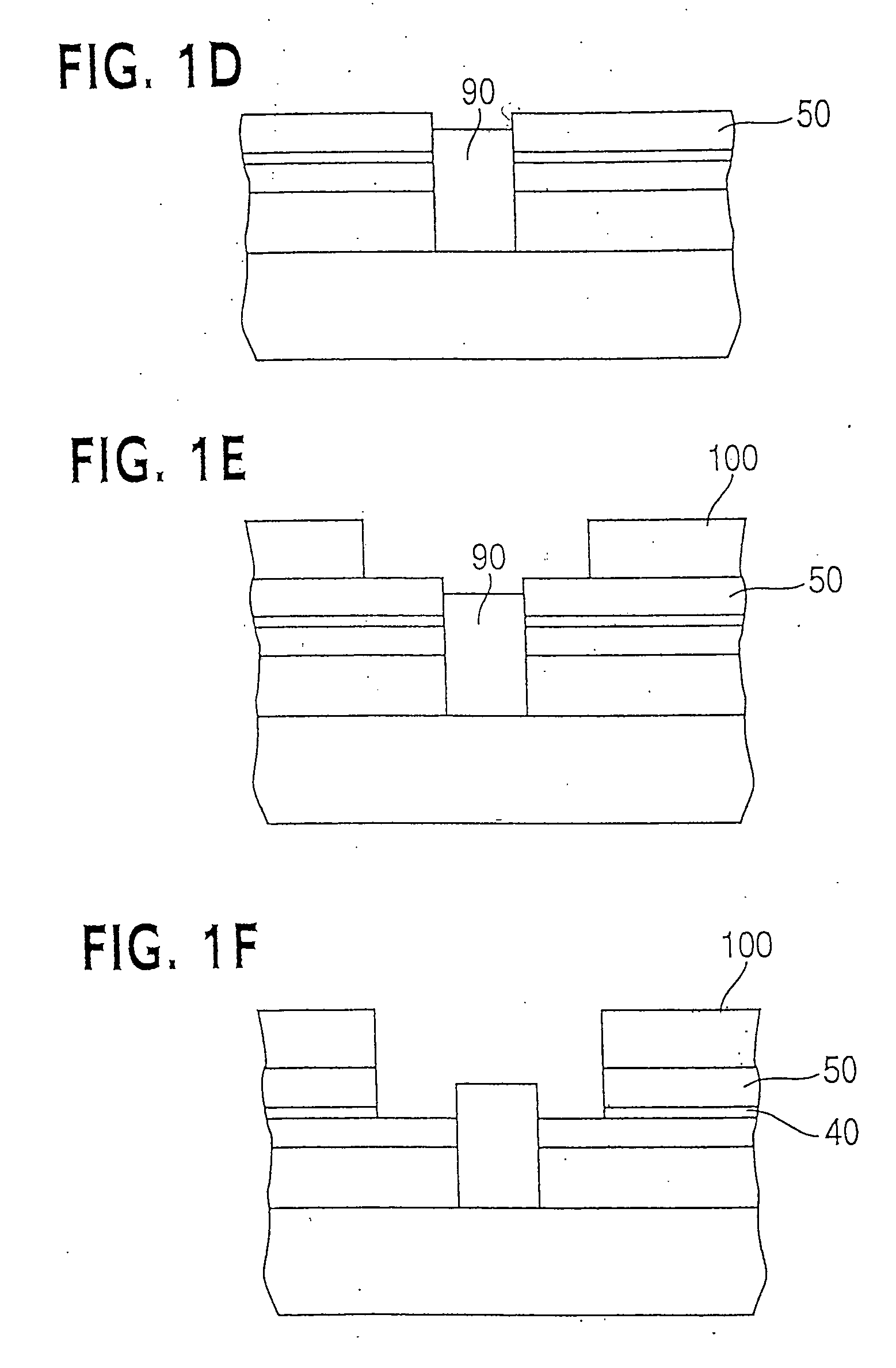
[0018] A method for forming a silicon-on-insulator FET according to a first preferred embodiment of the present invention will hereinafter be described in detail with reference to the accompanying drawings.

[0019]FIG. 1A-FIG. 1I are cross-sectional views showing a method for forming a silicon-on-insulator FET according to a first preferred embodiment of a present invention.

[0020] As shown in FIG. 1A, a silicon-on-insulator (SOI) structure is provided. Examples of the methods to form the SOI structure are called SIMOX (separation by implantation of oxygen) or a bonded wafer. The SOI structure is made up of a silicon substrate 10, an insulating layer 20, and a silicon layer 30. Then, a silicon oxide film 40 and a silicon nitride layer 50 are sequentially formed on the silicon layer 30. Then, a first resist pattern 60 is overlaid the silicon nitride layer 50. The first resist pattern 60 has an opening corresponding to a portion in which is formed a contact hole for a substrate-biasing...


PUM


Abstract

In a method for forming a silicon-on-insulator FET providing a contact to be given a fixed potential to a substrate, substrate-biasing between an SOI transistor and the silicon substrate is performed via a plug. As a result, the contact hole for the substrate-biasing does not need to pass through an insulating layer, a silicon layer, and an interlayer insulating layer. Therefore, the interlayer insulating layer can be made to have shallow depth. Ions can be implanted to the surface of the substrate via the contact hole for substrate biasing. As a result, contact holes for substrate-biasing can be formed without the contact holes for substrate-biasing causing an opening fault.

Description

CROSS REFERENCE TO RELATED APPLICATION [0001] This is a divisional application of application Ser. No. 10 / 445,859, filed May 28, 2003, which is a divisional application of application Ser. No. 09 / 962,190, filed Sep. 26, 2001, now U.S. Pat. No. 6,632,710, which are hereby incorporated by reference in their entirety for all purposes.BACKGROUND OF THE INVENTION [0002] 1. Field of the Invention [0003] The present invention generally relates to a method for forming a silicon-on-insulator FET, and more particularly, the present invention relates to the method for forming a silicon-on-insulator FET providing a contact to be given a fixed potential to a substrate reduction of contact resistance on a substrate having a SOI layer isolated with an insulating layer. [0004] This application is counterparts of Japanese application Serial Number 312351 / 2000, filed Oct. 12, 2000 and Japanese application Serial Number 118227 / 2001, filed Apr. 17, 2001, the subject matter of which is incorporated here...

Claims


Application Information

Patent Timeline
Patent Type & Authority Applications(United States)
IPC IPC(8): H01L21/84H01L21/762H01L21/74H01L21/768H01L21/8234H01L23/522H01L27/08H01L27/088H01L27/12H01L29/786
CPCH01L21/743H01L21/76802H01L21/76828H01L21/84H01L27/1203H01L29/66772H01L29/78648H01L29/78654
Inventor TAKAHASHI, AKIRA
Owner LAPIS SEMICON CO LTD
Features
  • R&D
  • Intellectual Property
  • Life Sciences
  • Materials
  • Tech Scout
  • Unparalleled Data Quality
  • Higher Quality Content
  • 60% Fewer Hallucinations
Learn More