Process for manufacturing a light emitting array

a technology of light-emitting arrays and manufacturing processes, which is applied in the manufacture of electrical discharge tubes/lamps, manufacturing tools, and manufacturing of electrical systems, etc., can solve the problems of one of the slowest and most expensive processes for producing a large number of optical elements

Inactive Publication Date: 2006-05-04
3M INNOVATIVE PROPERTIES CO
View PDF37 Cites 42 Cited by
  • Summary
  • Abstract
  • Description
  • Claims
  • Application Information

AI Technical Summary

Benefits of technology

[0004] The present application discloses methods of manufacturing shaped elements from a workpiece, where the workpiece is abraded to at least partially form channels that define an array of shaped elements. Surfaces of the channels are polished to optical quality with a patterned abrasive.

Problems solved by technology

However, lapping is one of the slowest and most expensive processes for producing a large number of optical elements, especially for ceramics with high thermal conductivity, such as diamond, silicon carbide, and sapphire.
In addition, individually lapped shaped elements must be handled individually, which is difficult.

Method used


Image

  • Process for manufacturing a light emitting array
  • Process for manufacturing a light emitting array
  • Process for manufacturing a light emitting array

Examples


Embodiment Construction

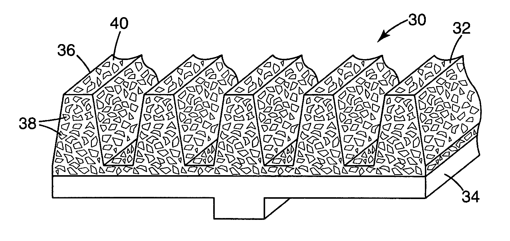
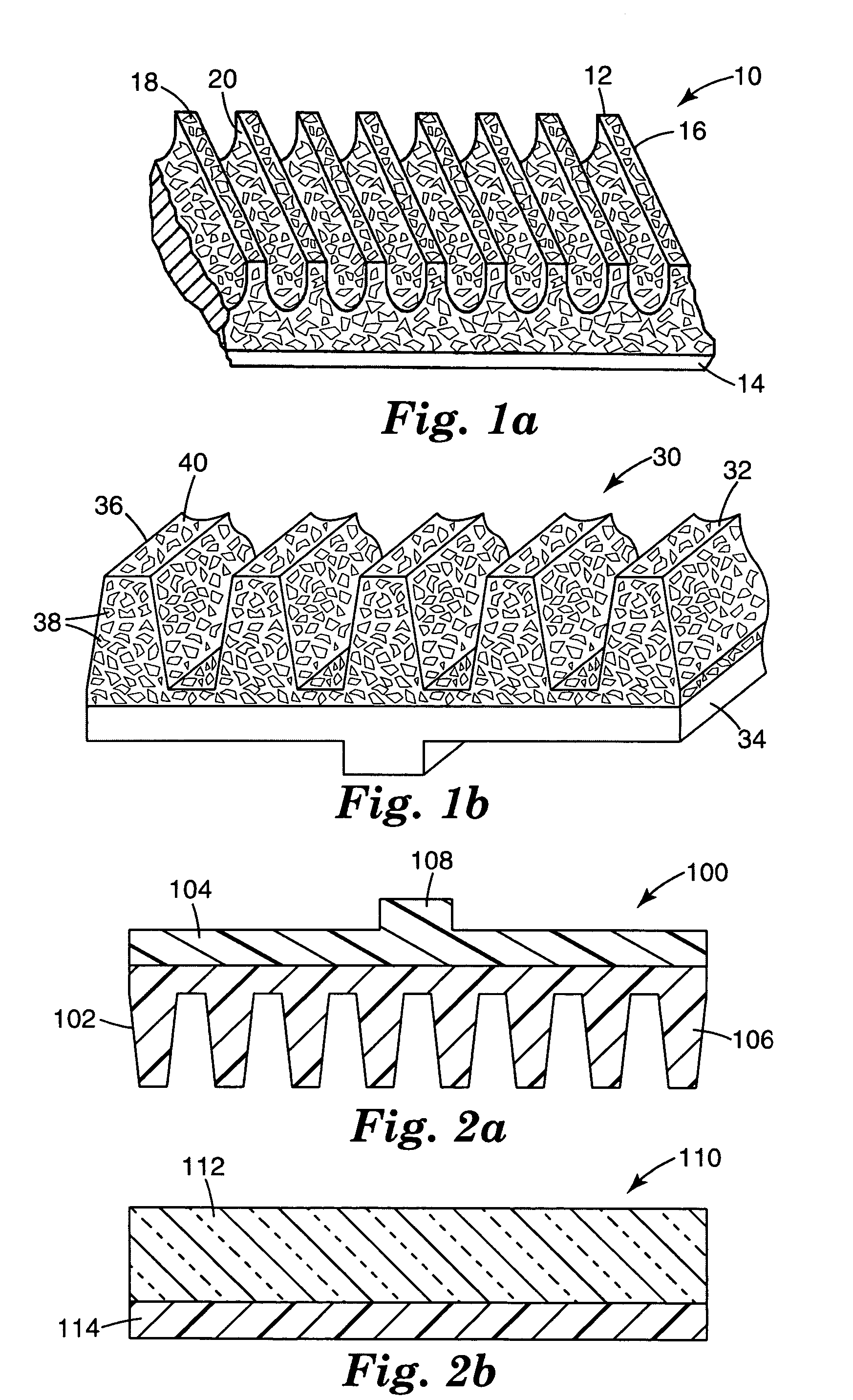
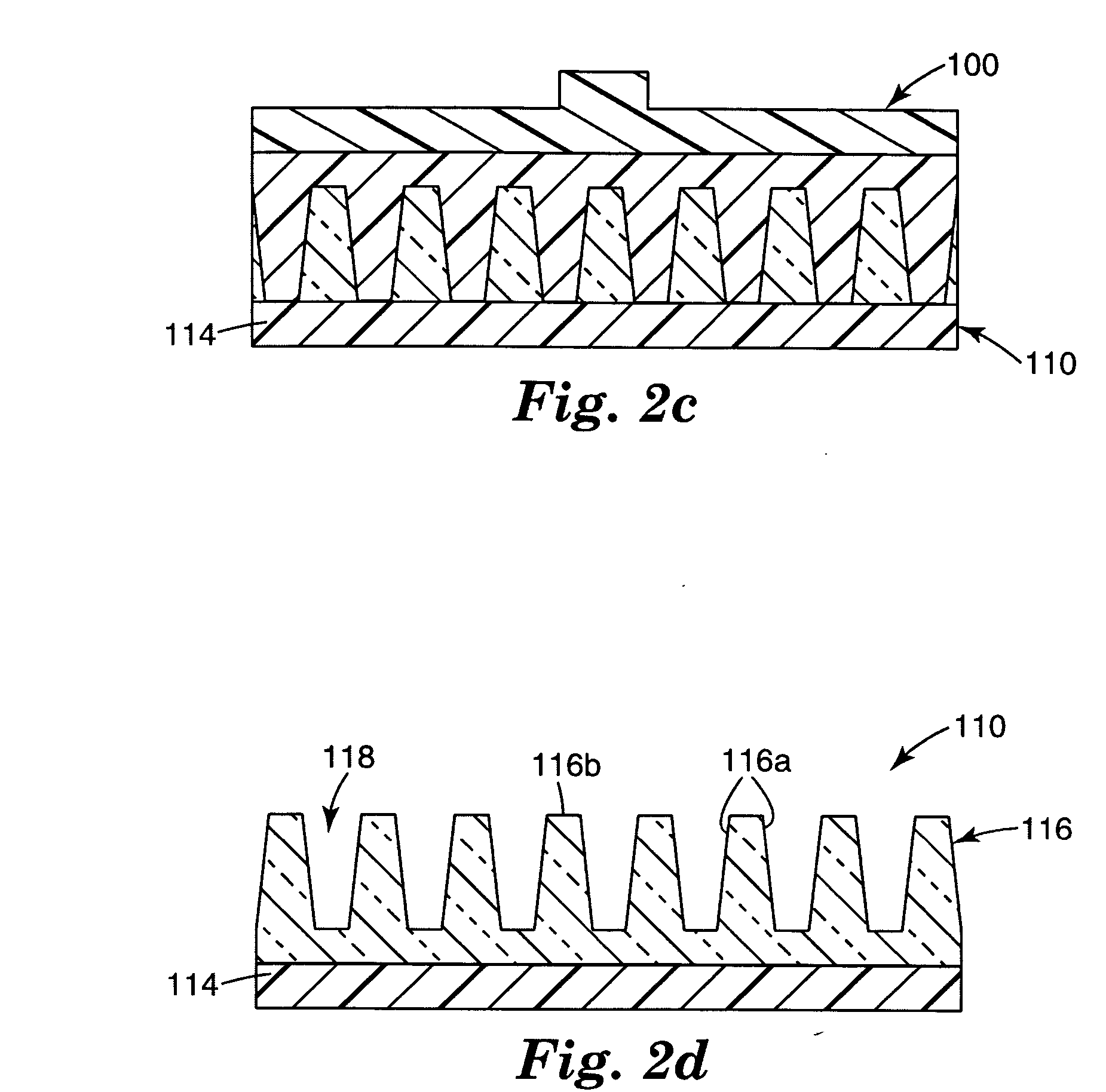
[0013]FIGS. 1a and 1b show representative embodiments of patterned abrasive 10, 30 for abrading substrate material to form an array of individual optical and / or semiconductor elements. As used herein, abrading may include abrading and polishing substrate material simultaneously, however, polishing may occur as a separate step. In addition, as used herein in regard to elements or shaped elements, “individual” and “singulated” refers to elements that are identifiable units but that are not necessarily detached from other elements. Likewise, singulating refers to forming identifiable units, which are not necessarily detached from one another. As shown, patterned abrasives 10, 30 include working surfaces 12, 32 and abackings 14, 34. Working surfaces 12, 32 includes protrusions 16, 36, particles 18, 38, and binder 20, 40.

[0014] Patterned abrasive 10, 30 is formed by applying a composite of particles 18, 38 dispersed in binder 20, 40 to backing 14, 24. Backing 14, 24 may be materials suc...


PUM

PropertyMeasurementUnit
thermal diffusivityaaaaaaaaaa
heightaaaaaaaaaa
heightaaaaaaaaaa

Abstract

A method for fabricating a light emitting array utilizes a precisely shaped patterned abrasive to abrade optical material. One or more patterned abrasives contact and abrade along one or more intersecting axes of the optical material. The resulting precisely shaped and located optical elements are aligned with and bonded to an array of light sources.

Description

RELATED PATENT APPLICATIONS [0001] The following co-owned and pending U.S. patent applications are incorporated by reference: “PROCESS FOR MANUFACTURING OPTICAL AND SEMICONDUCTOR ELEMENTS”, Attorney Docket No. 60203US002. BACKGROUND OF THE INVENTION [0002] The present invention relates to a process for manufacturing an array of shaped elements, such as optical elements and semiconductor elements. [0003] Optical elements (i.e. shaped bodies of inorganic or organic material and faceted along at least one plane, the shaped bodies reflecting, refracting, and absorbing light and / or conducting heat) and semiconductor elements having at least one dimension of less than a few millimeters are currently fabricated by a number of processes. These processes include molding, lapping individual elements, casting the optical elements from a sol-gel followed by sintering, microreplication, and processes using surface tension or shrinkage to form desired shapes. Of these processes, only lapping allo...

Claims


Application Information

Patent Timeline
Patent Type & Authority Applications(United States)
IPC IPC(8): H01J9/00H01J9/24H01L33/20H01L33/58
CPCB24B13/02H01L33/20H01L33/58H01L2924/0002H01L2924/00B24D2203/00
Inventor OUDERKIRK, ANDREW J.LEATHERDALE, CATHERINE A.BENSON, OLESTER JR.
Owner 3M INNOVATIVE PROPERTIES CO
Why Eureka
Try Eureka