Amplifier with low pass filter feedback

a low-pass filter and amplifier technology, applied in the direction of amplifiers, electrical apparatus, pulse automatic control, etc., can solve the problem that the capacitors require a lot of space on the silicon chip, and achieve the effect of extending the useable frequency rang

Active Publication Date: 2006-05-11
NAT SEMICON GERMANY
View PDF2 Cites 19 Cited by
  • Summary
  • Abstract
  • Description
  • Claims
  • Application Information

AI Technical Summary

Benefits of technology

[0009] In the feedback unit according to the invention, instead of a large capacitor an additional amplifier stage is provided, between whose inputs and outputs at least one Miller capacitor of comparatively small dimensions is connected. Since the amplifier stage amplifies an applied voltage by an amplification factor, hereinafter referred to as A2, and since to this extent a significantly higher voltage is present at the connections of the Miller capacitor, the relatively small-dimensioned Miller capacitor can store a charge quantity which corresponds to the charge of a capacitor that is larger by the factor (1+A2). Interconnecting an amplifier stage with at least one small-dimensioned capacitor thus has the same effect as a significantly larger capacitance. The space requirement of the additional amplifier stage is relatively small so that by utilising the Miller effect a significant reduction in the silicon area required by the lowpass can be achieved. In this way the feedback unit for offset suppression can be implemented so that it is smaller and more cost-effective than up to now.
[0025] Preferably, the additional amplifier stage or attenuation stage is implemented as a transconductance stage whose output current works against terminating resistors of input lines of the amplifier. By means of a transconductance stage it becomes possible to very precisely adjust the amplification or attenuation A3. The output current of the transconductance stage causes an additional voltage drop at the terminating resistors. This results in superposition of the input signal with this voltage drop caused by the feedback signal. The superposition signal generated in this way, which comprises a significantly reduced steady component, is then fed to the amplifier.

Problems solved by technology

Such solutions are associated with a disadvantage in that the required capacitors require a lot of space on the silicon chip.

Method used


Image

  • Amplifier with low pass filter feedback
  • Amplifier with low pass filter feedback
  • Amplifier with low pass filter feedback

Examples


Embodiment Construction

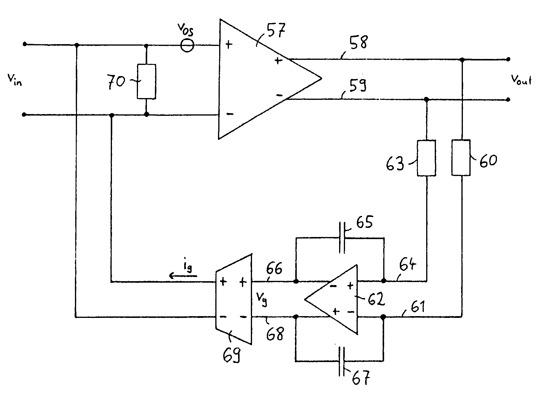
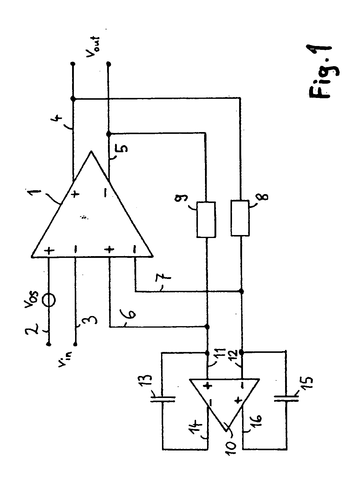
[0033]FIG. 1 shows a first embodiment of an amplifier according to the invention. Amplifiers are associated with a problem in that an input offset vos is amplified at the same time, which results in an undesired steady component in the output signal of the amplifier. In extreme cases an amplifier can even be overloaded by its own offset. This problem occurs in particular in the case of broadband amplifiers with bandwidths of for example 8.5 GHz, because due to the high-frequency signal fractions the transistors have to be very small. In such amplifiers the statistical fluctuations in the transistor threshold voltages cause an input offset of up to 10 mV. With amplification of approximately 30 dB, this would lead to a steady component of approximately 300 mV at the output, i.e. approximately half of the dynamic range.

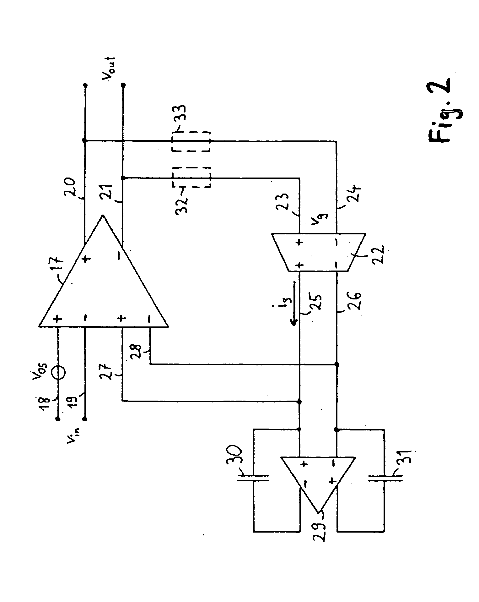
[0034] The amplifier 1 shown in FIG. 1 comprises first inputs 2, 3, to which the input signal vin is applied. The input signal vin is amplified by the amplifier 1 accor...


PUM


Abstract

An amplifier is described which amplifies an input signal according to a defined amplification factor, and which generates an output signal. To reduce an offset fraction of the output signal the amplifier comprises a feedback path which has lowpass characteristics and which returns the output signal in a lowpass-filtered state to an input of the amplifier. The feedback path comprises an amplifier stage as well as at least one Miller capacitance connected between an input and an output of the amplifier stage.

Description

BACKGROUND TO THE INVENTION [0001] 1. Field of the Invention [0002] The invention relates to an amplifier and a feedback unit for reducing an offset fraction in the output signal of the amplifier. [0003] 2. Description of the State of the Art [0004] In the context of amplifiers a problem can arise in that an input offset of the amplifier (and also an offset of the input signal) can be amplified at the same time by the amplifier so that the output signal of the amplifier comprises an undesirable steady component. This problem is encountered in particular in the case of amplifiers that are designed for amplifying high-frequency signal components. In such broadband amplifiers the transistors have to be of very small dimensions so that frequency components, for example in the gigahertz range, can be amplified. This relatively small dimensioning of the transistors results in significant fluctuations in the transistor threshold voltages, and consequently a significant input offset results...

Claims


Application Information

Patent Timeline
Patent Type & Authority Applications(United States)
IPC IPC(8): H03F1/36
CPCH03F3/45H03F1/34
Inventor EBNER, CHRISTIAN
Owner NAT SEMICON GERMANY
Why Eureka
Try Eureka