Electronic device package and electronic equipment

a technology of electronic equipment and electronic devices, applied in semiconductor devices, semiconductor/solid-state device details, instruments, etc., can solve the problems of increasing the size of the wiring region on the substrate, the lower limit value of the array pitch of the electrodes on the substrate being large, and the inability to correspond to the pitch of the wiring upon the substrate (the substrate electrode) being large, etc., to achieve the effect of reducing the size and weight of the electronic devi

Inactive Publication Date: 2006-05-18
SEIKO EPSON CORP
View PDF6 Cites 29 Cited by
  • Summary
  • Abstract
  • Description
  • Claims
  • Application Information

AI Technical Summary

Benefits of technology

[0026] It is possible to anticipate reduction of size and weight of this electronic device, due to its electronic device package having been made more compact.

Problems solved by technology

However, even if the pitch of the terminal electrodes upon the electronic device is narrowed down, it often happens that the pitch of the wiring upon the substrate (the substrate electrode) cannot correspond thereto.
In other words, due to various limitations, there is a tendency for the lower limit value for the array pitch of the electrodes upon the substrate to be large, as compared with that for the electrodes upon the electronic device.
This fact can easily lead to increase of the size of the wiring region upon the substrate, due to the requirements for extending the wiring and the like, and this can constitute a hindrance to making the substrate more compact.

Method used


Image

  • Electronic device package and electronic equipment
  • Electronic device package and electronic equipment
  • Electronic device package and electronic equipment

Examples


Embodiment Construction

[0039] In the following, preferred embodiments of the present invention will be described with reference to the drawings.

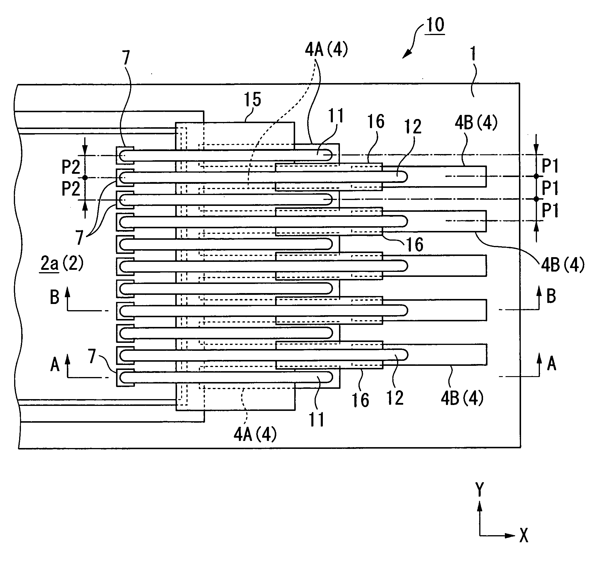
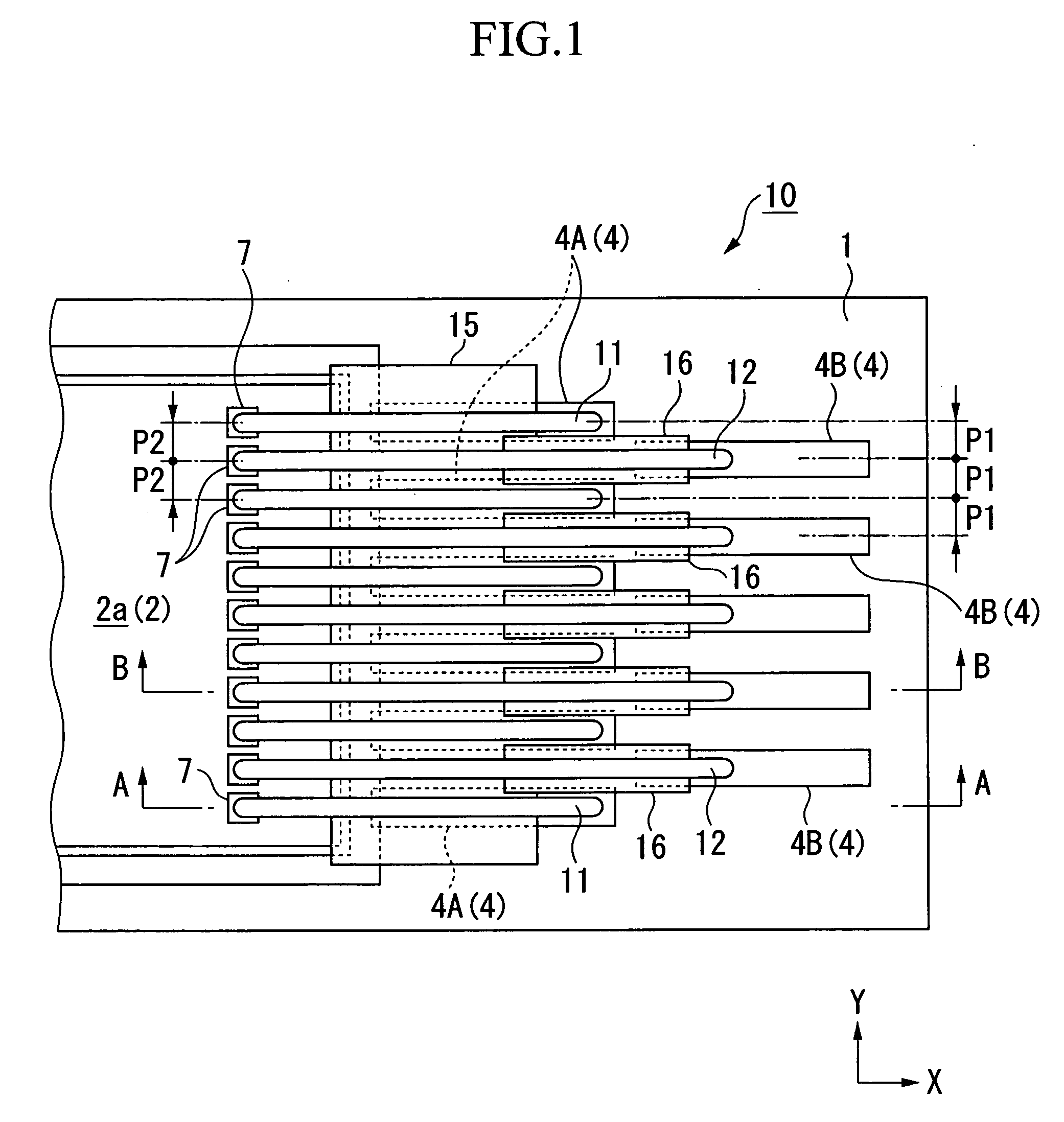
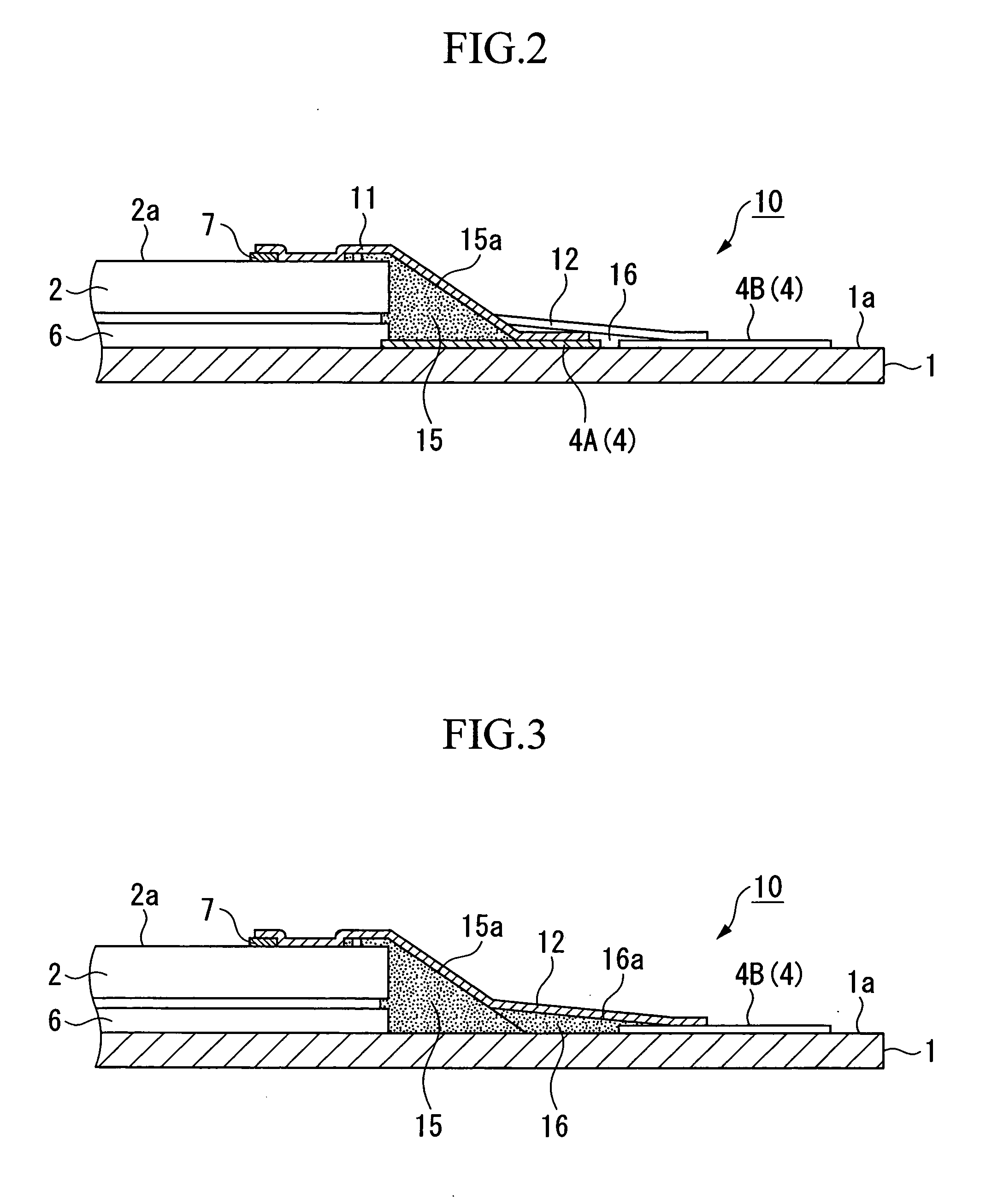
[0040]FIG. 1 is a partial plan view showing a preferred embodiment of the electronic device package according to the present invention.

[0041] As shown in FIG. 1, in this electronic device package 10, a chip component (an electronic device) 2 is face-up bonded upon a substrate 1, and it has a structure in which electrodes 7 of the chip component 2 (device electrodes 7), and electrodes 4 of the substrate 1 (substrate electrodes 4) are electrically connected together.

[0042] The substrate 1 is a multi-layer or single layer wiring substrate upon which a wiring pattern is formed, and its main body may be rigid or may be flexible. In this wiring pattern, there are formed a plurality of electrode terminals (the substrate electrodes 4). This plurality of substrate electrodes 4, apart from being formed by a plating method or a stud method or the like, may also be formed ...


PUM


Abstract

This electronic device package includes a substrate upon which an electronic device is mounted, a plurality of device electrodes which are formed upon an electronic device, a plurality of substrate electrodes which are formed upon the substrate, and a plurality of connection lines, formed by a liquid drop ejection method, each of which electrically connects together one of the plurality of device electrodes and one of the plurality of substrate electrodes. The plurality of substrate electrodes are arranged in a staggered configuration.

Description

BACKGROUND OF THE INVENTION [0001] 1. Field of the Invention [0002] The present invention relates to an electronic device package, and to an electronic equipment. [0003] Priority is claimed on Japanese Patent Application No. 2004-331962, filed Nov. 16, 2004, the content of which is incorporated herein by reference. [0004] 2. Description of Related Art [0005] From the past, as a technique for mounting an electronic device such as a semiconductor chip (an IC chip) or the like upon a substrate, in order electrically to connect together a terminal electrode on one surface of the electronic device (a device electrode) and a wiring pattern upon the substrate, the so called wire bonding technique has been widely used (for example, refer to Japanese Unexamined Patent Application, First Publication No. 2004-221257). [0006] Apart from this technique, as a technique related to the above described electrical connection, there is a technique in which an electrically conductive member is sandwich...

Claims


Application Information

Patent Timeline
Patent Type & Authority Applications(United States)
IPC IPC(8): H01L23/48
CPCH01L23/49805H01L2224/25175H01L23/49827H01L23/49838H01L24/24H01L24/25H01L24/82H01L24/83H01L2224/24011H01L2224/24051H01L2224/24226H01L2224/24998H01L2224/291H01L2224/76155H01L2224/83801H01L2224/83851H01L2224/92H01L2924/01002H01L2924/01013H01L2924/01015H01L2924/01018H01L2924/01029H01L2924/01033H01L2924/01046H01L2924/01054H01L2924/01074H01L2924/01078H01L2924/01079H01L2924/01082H01L2924/07802H01L2924/0781H01L2924/12044H01L2924/14H01L2924/19041H01L2924/19042H01L2924/19043H01L2924/30107H01L23/49811H01L2224/73267H01L2224/82102H01L2224/293H01L2224/2929H01L2224/82007H01L24/76H01L2924/01005H01L2924/01006H01L2924/01047H01L2224/32225H01L2224/83H01L2224/82H01L2924/00014H01L2224/05554H01L21/50
Inventor KUROSAWA, HIROFUMI
Owner SEIKO EPSON CORP
Why Eureka
Try Eureka