Light emitting screen structure and image forming apparatus

a technology of light emitting screen and image forming apparatus, which is applied in the direction of screens, discharge tubes, cathode-ray/electron beam tube circuit elements, etc. it can solve the problems of destroying causing the discharge tube to destruct the electron emitting device, and uneven luminance of 50% at maximum, so as to prevent an electrical destruction and ensure durability.

Inactive Publication Date: 2006-05-18
CANON KK
View PDF15 Cites 32 Cited by
  • Summary
  • Abstract
  • Description
  • Claims
  • Application Information

AI Technical Summary

Benefits of technology

[0018] An object of the present invention is to provide a light emitting screen structure for further suppressing a discharge current, thereby relaxing an influence of an abnormal discharge to an electron emitting device and realizing a satisfactory durability and a long life in an image forming apparatus. In particular, the present invention is to provide a light emitting substrate structure capable of preventing an electrical destruction between anode electrodes without increasing a distance between the adjacent anode electrodes.

Problems solved by technology

In such configuration, however, as a high electric field is inevitably formed between the opposed electrodes, a discharge may be generated to destruct the electron emitting device.
The destruction by discharge is assumed to be caused by a large current concentrated in a single position within a short time resulting in a heat generation which destructs the electron emitting device, or by an instantaneous increase in the voltage on the electron emitting device, leading to the destruction of the electron emitting device.
However, in case of connecting devices of 500 units in the vertical direction by 1000 units in the horizontal direction with row and column wirings and driving these elements in a line-sequential mode, about 1000 devices are simultaneously turned on and such method leads to following drawbacks.
As a result, there will result an unevenness in the luminance of 50% at maximum.
Such discharge current leads to the destruction of the devices, so that the configuration of FIG. 7 cannot provide a sufficient solution to the drawback even if the aforementioned unevenness in luminance is absent.

Method used


Image

  • Light emitting screen structure and image forming apparatus
  • Light emitting screen structure and image forming apparatus
  • Light emitting screen structure and image forming apparatus

Examples


example 1

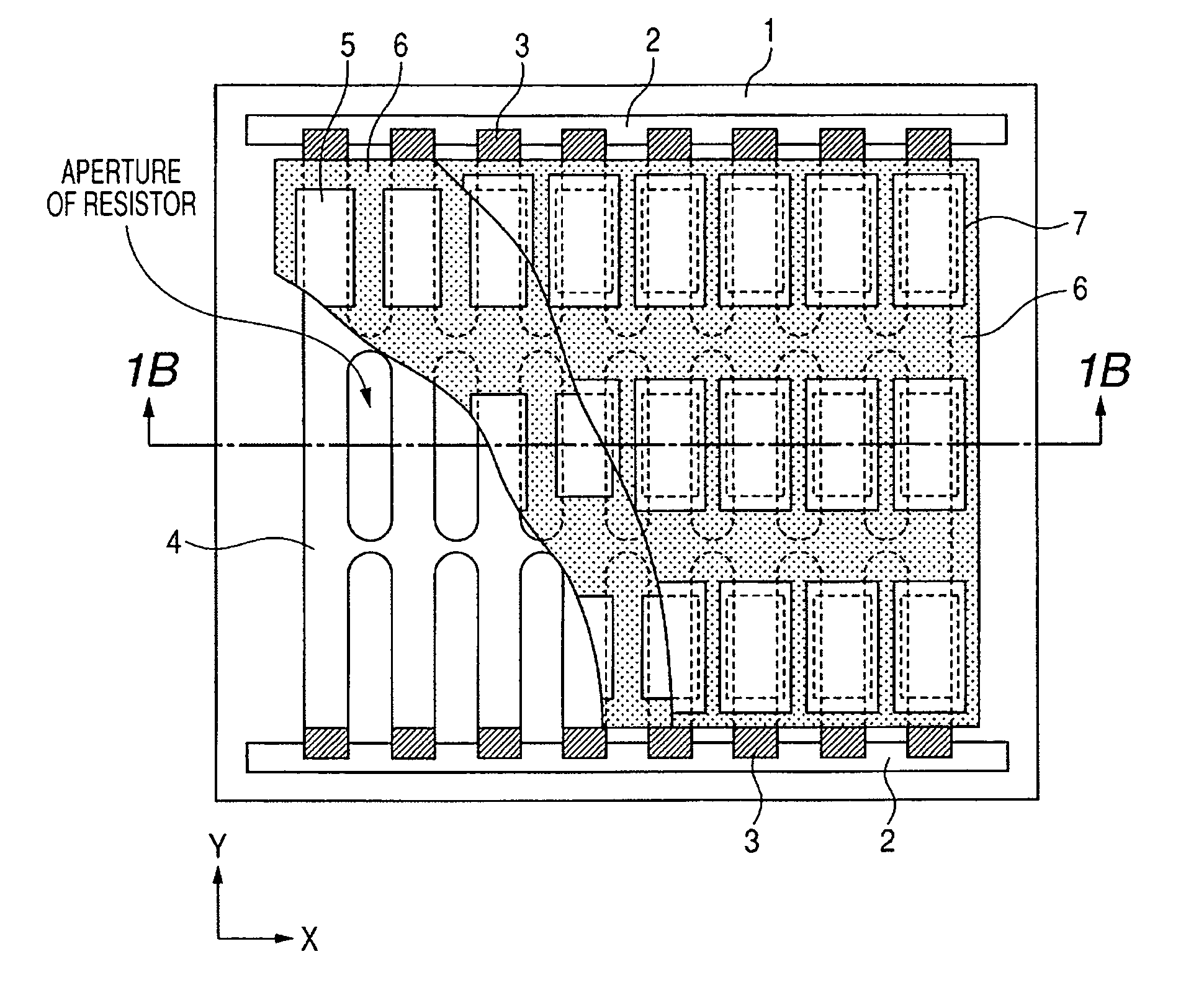
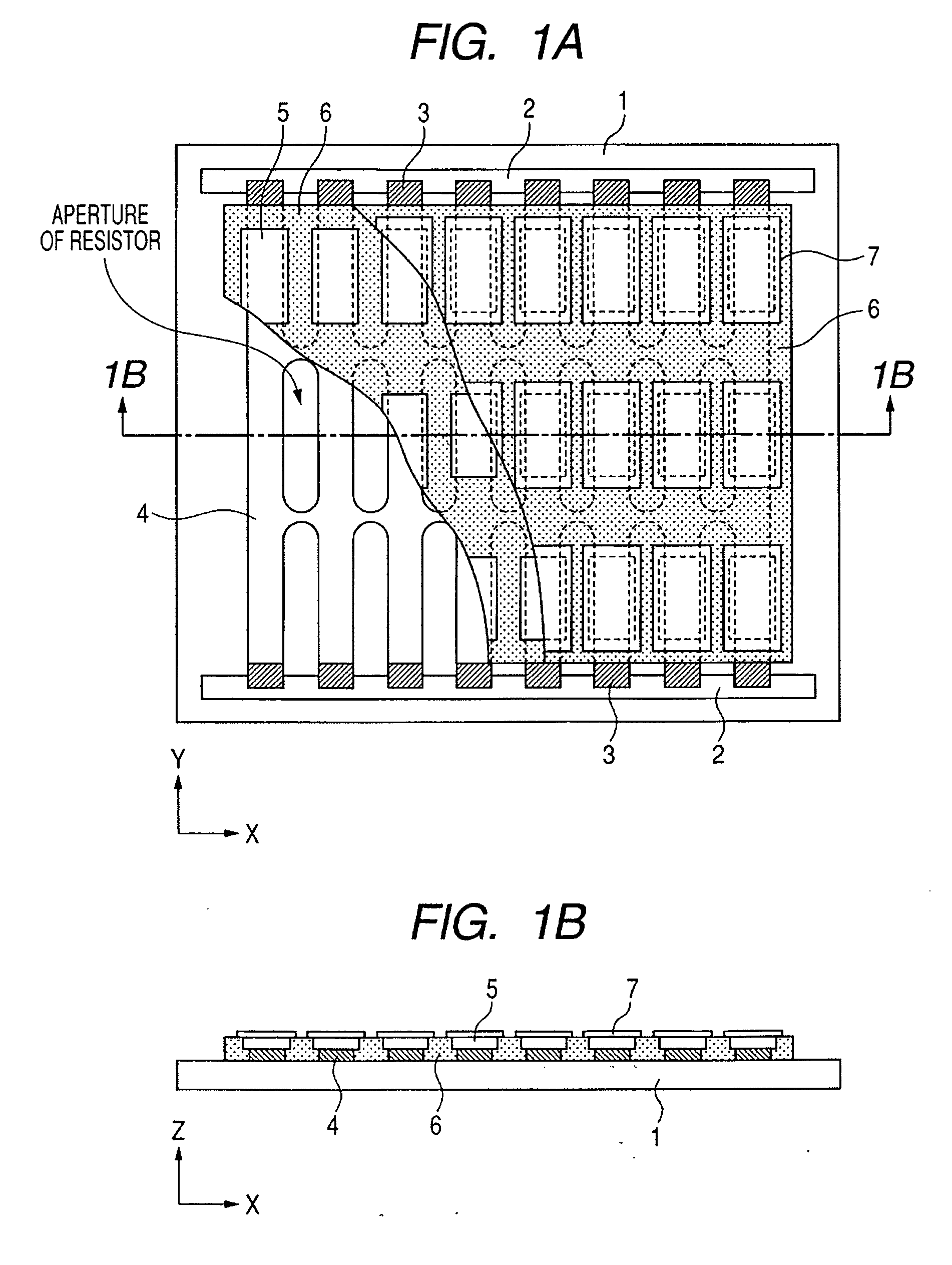
[0062] A light emitting substrate of a configuration shown in FIGS. 1A and 1B was prepared in a following procedure.

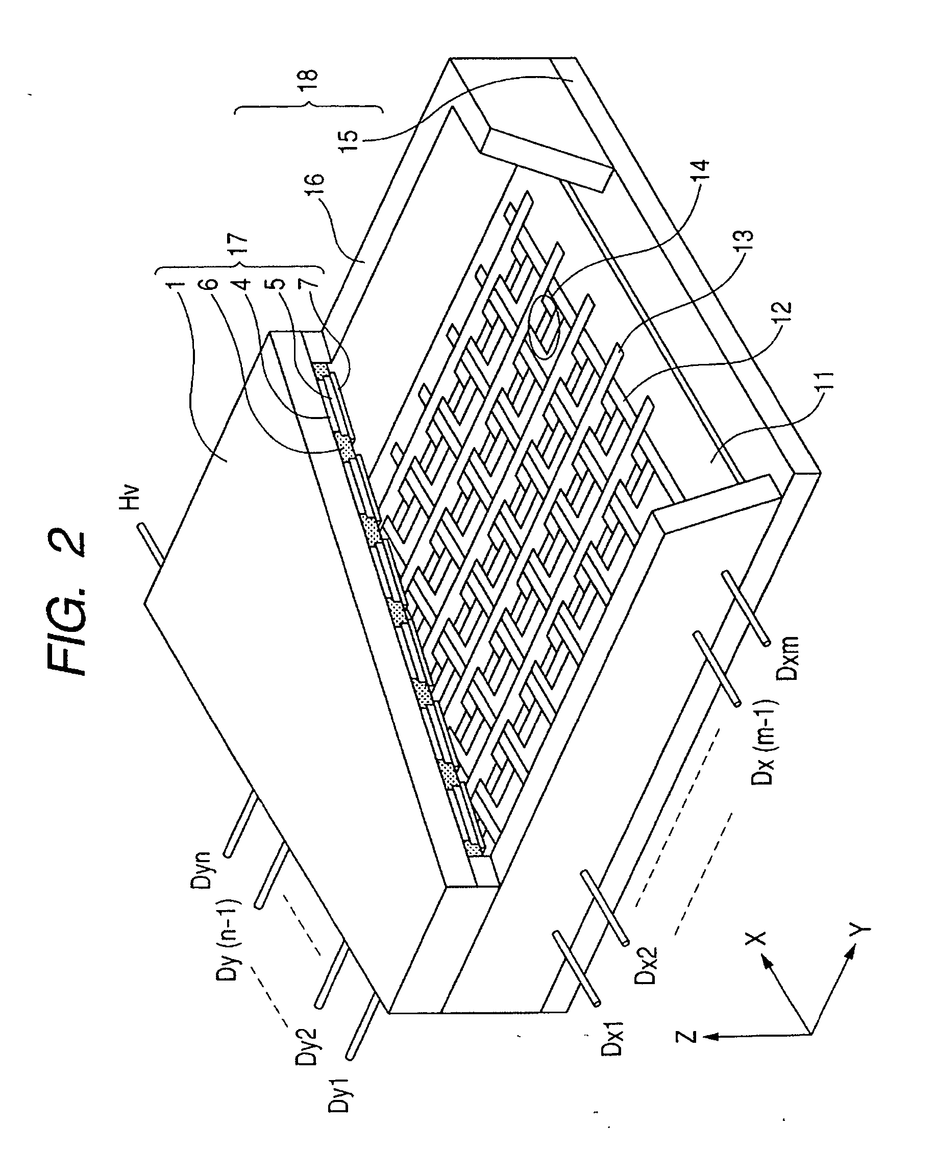
[0063] On a glass substrate 1, an ITO film was formed on an entire upper surface, and was formed into a lattice-shaped pattern by a photolithographic process to obtain a resistor member 4. Then patterned NiO films were formed as connecting resistors 3. Then a common electrode 2 was formed with an Ag paste, so as to be in contact with all the connecting resistors 3. Then, on the patterned ITO film, NP-7803 (manufactured by Noritake Kizai Co.) was printed as a black member 6, then red, green and blue phosphors 5 were coated and baked. Finally island-shaped metal backs 7 were formed by a vacuum evaporation method on the phosphor 5.

[0064] In the present example, there was employed a glass substrate PD200, manufactured by Asahi Glass Co., of a thickness of 2.8 mm. Also in the resistor member 4, the ITO film extending in the Y-direction had a width of 100 μm and a thicknes...

example 2

[0071] A light emitting substrate of a configuration shown in FIGS. 3A and 3B was prepared. This example was similar to Example 1 except that three phosphors 5 of red, green and blue arranged in succession in the X-direction were collectively covered by a single metal back 7.

[0072] In the present example, the Y-direction stripe portion of the ITO resistor extending in the Y-direction had a width of 100 μm and a thickness of 100 nm, and the ITO film was regulated to a sheet resistance of 30 kΩ / square so as to obtain a resistance of about 120 kΩ between the metal backs 7 adjacent in the Y-direction. Also the ITO film extending in the X-direction had a width of 50 μm so as to obtain a resistance (individual resistance) of about 800 kΩ between the metal backs adjacent in the X-direction. Also a crossing part of the lattice pattern of the resistance member 4 had a curvature of a radius of 50 μm, matching the narrower stripe width in the X-direction.

[0073] In this manner there was obtai...

example 3

[0078] A light emitting substrate of a configuration shown in FIGS. 4A and 4B was prepared. This example was similar to Example 2 except that the resistor member 4 was positioned under the black member 6 and that two Y-direction stripe portions of the resistor member 4, extending in the Y-direction, were provided per metal back.

[0079] In the present example, in the ITO resistor member, the Y-direction stripe portion had a width of 50 μm, and the ITO film was regulated to a sheet resistance of 30 kΩ / square so as to obtain a resistance of about 120 kΩ between the metal backs 7 adjacent in the Y-direction. Also the X-direction stripe portion of the ITO film had a width of 30 μm so as to obtain a resistance (individual resistance) of about 800 kΩ between the metal backs adjacent in the X-direction. Also a crossing part of the lattice pattern of the resistance member 4 had a curvature of a radius of 50 μm, matching the narrower stripe width in the X-direction.

[0080] An image forming ap...


PUM


Abstract

In a flat type image forming apparatus formed by electron emitting devices, the invention is to provide a light emitting substrate, capable of relaxing influence of an abnormal discharge on the electron emitting devices. On a glass substrate 1, a resistor member 4 extending in X- and Y-direction, and a black member 6 extending in X- and Y-directions are formed. Phosphors 5 are positioned in apertures of the black member 6, and are covered by metal backs 7 divided in X- and Y-directions. The metal backs 7 and the resistor member 4 are electrically connected through the black member 6, and the resistance between the metal backs 7 is defined by the resistor member 4 in the Y-direction in which the adjacent metal backs 7 have a wider gap than in the X-direction.

Description

BACKGROUND OF THE INVENTION [0001] 1. Field of the Invention [0002] The present invention relates to a light emitting screen structure (light emitting substrate) for constituting an image forming apparatus such as an image display apparatus in combination with an electron emitting device, and to an image forming apparatus utilizing such light emitting substrate. [0003] 2. Related Background Art [0004] An electron emitting apparatus utilizing an electron emitting device has been applied for example to an image forming apparatus. For example, there is known a flat type electron beam display panel, formed by arranging an electron source substrate provided with a plurality of cold cathode electron emitting devices, and an anode substrate provided with a metal back or a transparent electrode for accelerating electrons emitted from the electron emitting devices, and a phosphor in a mutually opposed relationship and by evacuating a gap between such substrates. The flat type electron beam d...

Claims


Application Information

Patent Timeline
Patent Type & Authority Applications(United States)
IPC IPC(8): H01J63/04
CPCH01J29/085H01J29/96H01J31/127H01J2329/28H01J29/28H01J31/12
Inventor SUZUKI, NORIHIROYAMAZAKI, KOJI
Owner CANON KK
Why Eureka
Try Eureka