Plasma display device and driving method with reduced displacement current

a technology of a display device and a driving method, which is applied in the direction of instruments, static indicating devices, etc., can solve the problems of dc pdp, degraded light emission efficiency by sustain discharge, and requires a resistor for limiting current, so as to achieve the effect of improving light emission efficiency

Inactive Publication Date: 2006-05-18
SAMSUNG SDI CO LTD
View PDF7 Cites 18 Cited by
  • Summary
  • Abstract
  • Description
  • Claims
  • Application Information

AI Technical Summary

Benefits of technology

[0008] The present invention provides a plasma display device and a drivi...

Problems solved by technology

The DC PDP has a disadvantage in that it requires a resistor for limiting the current.
However, the positive wall charges are distributed between the sustain electrode X an...

Method used


Image

  • Plasma display device and driving method with reduced displacement current
  • Plasma display device and driving method with reduced displacement current
  • Plasma display device and driving method with reduced displacement current

Examples


first embodiment

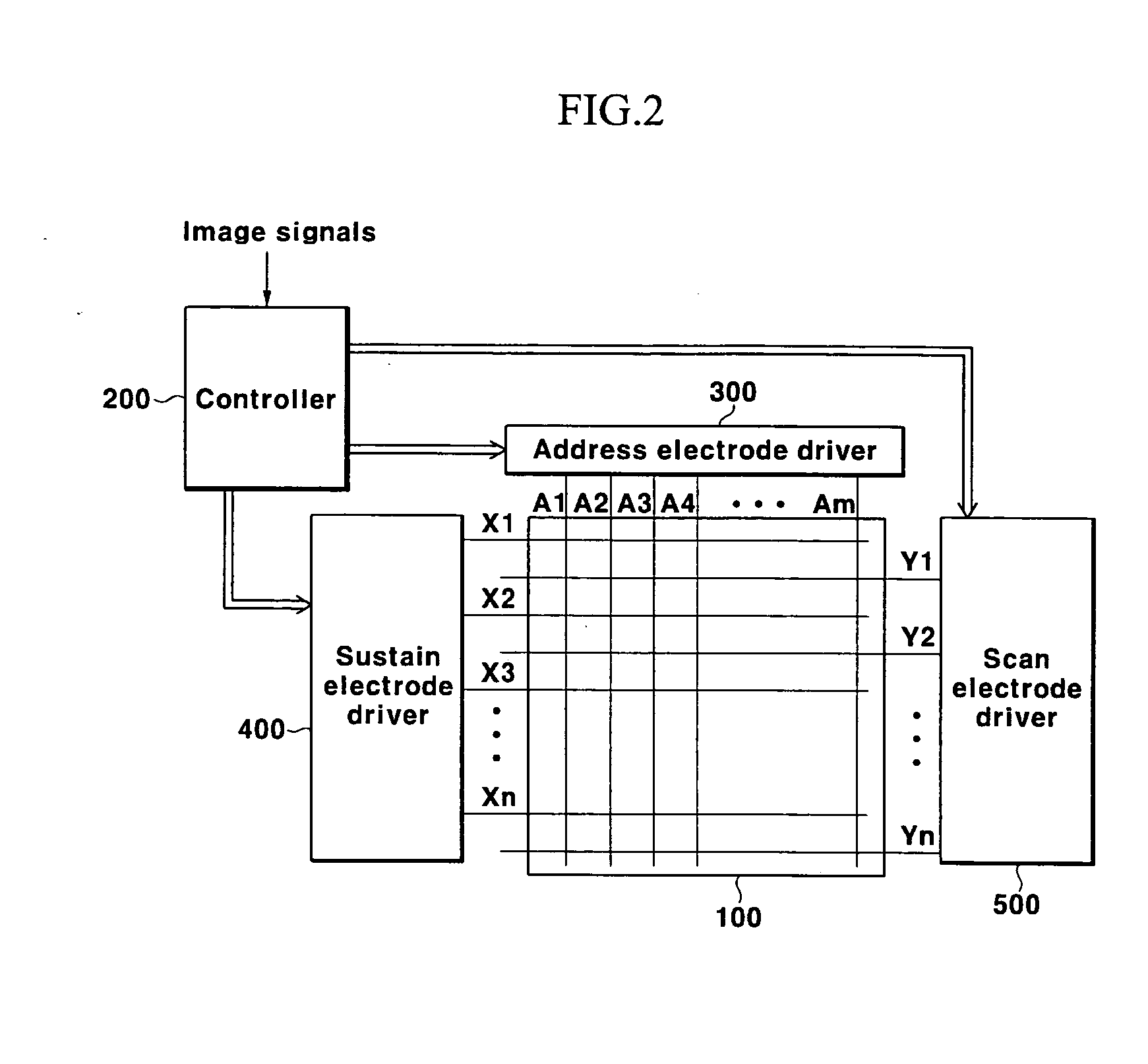
[0025]FIG. 3 shows a driving waveform for a plasma display device according to the present invention. The figure includes the driving waveforms applied to the address electrodes A1 to Am, the sustain electrodes X1 to Xn, and the scan electrodes Y1 to Yn during each subfield. The subsequent description is provided with reference to a discharge cell. Wall charges represent charges formed on the wall, i.e., a dielectric layer, of discharge cells near each electrode and accumulated at the electrode. The terms “formed,”“accumulated,” or “piled” are used for the accumulation of wall charges on a dielectric coating an electrode while the wall charges do not actually contact the electrode. A wall voltage represents a potential difference between the walls of the discharge cells arising due to the accumulation of wall charges.

[0026] A reset period is divided into a rising period and a falling period. During the rising period of the reset period, a voltage at the scan electrode Y is gradually...

second embodiment

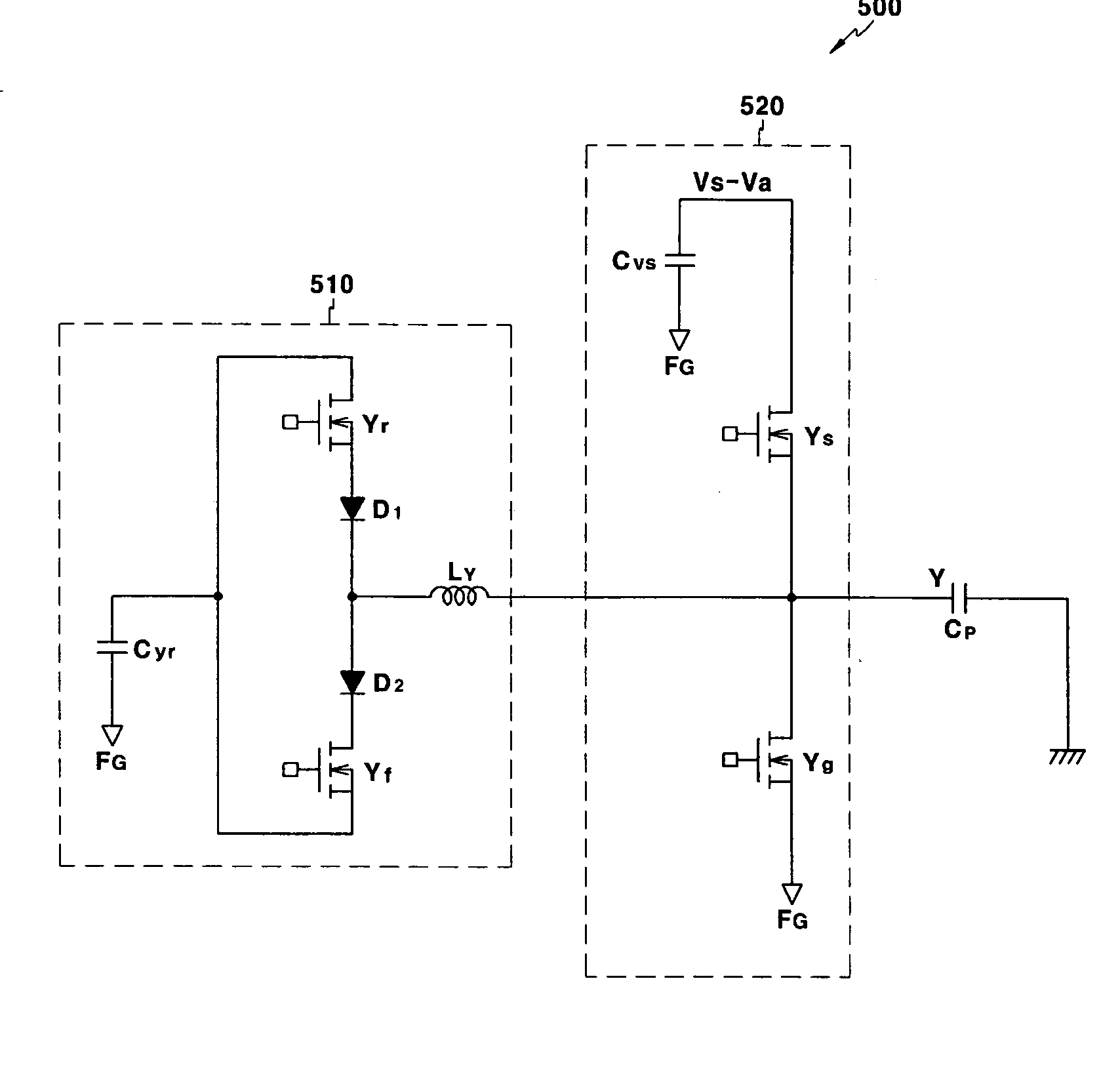
[0053] As shown in FIG. 10, a sustain discharge pulse applied to the scan electrode Y and the sustain electrode X during the sustain period is increased from the reference voltage to the voltage Vs-Va and subsequently to the voltage Vs, and then decreased from the voltage Vs to the voltage Vs-Va and further decreased from voltage Vs-Va back to the reference voltage. The voltage at the address electrode A is increased from the reference voltage to the voltage Va and is then decreased from the voltage Va back to the reference voltage during the period in which the sustain pulse is increased from Vs-Va to Vs and then decreased from Vs to Vs-Va. Accordingly, in the present invention, the voltage Va is applied to the address electrode A by using LC resonance of the power recovery circuit 310, and the sustain pulse is not steeply increased from the voltage Vs-Va to the voltage Vs, but is rather increased with the gradient of LC resonance.

[0054] A method for applying the driving waveforms ...


PUM


Abstract

A plasma display device and a driving method thereof. A scan electrode driver (or a sustain electrode driver) uses a power source for supplying the voltage Vs-Va to increase the initial voltage to the voltage Vs-Va and uses an address voltage output by an address electrode driver to increase the voltage Vs-Va to the voltage Vs to thus apply a sustain discharge pulse during a sustain period. Therefore, the voltage used by a driver for applying the sustain discharge pulse is reduced by using a voltage output by the address driver to apply the sustain pulse voltage.

Description

CROSS-REFERENCE TO RELATED APPLICATION [0001] This application claims priority to and the benefit of Korean Patent Application 10-2004-0093432 filed in the Korean Intellectual Property Office on Nov. 16, 2004, the entire content of which is incorporated herein by reference. BACKGROUND OF THE INVENTION [0002] 1. Field of the Invention[0003] The present invention relates to a plasma display device including a plasma display panel (PDP) and a driving method of the plasma display device and, more particularly, to circuits required for generating waveforms of the driving method. [0004] 2. Description of the Related Art [0005] Recently, flat panel displays, such as liquid crystal displays (LCDs), field emission displays (FEDs), and plasma display devices have been actively developed. Plasma display devices have features of high luminance, high luminous efficacy, and wide viewing angle. Accordingly, plasma display devices are highlighted as substitutes for conventional cathode ray tubes (C...

Claims


Application Information

Patent Timeline
IPC IPC(8): G09G3/10G09G3/20G09G3/288G09G3/291G09G3/292G09G3/294G09G3/296G09G3/298
CPCG09G3/294G09G3/2965G09G2310/0267G09G3/296
Inventor KIM, JOON-YEON
Owner SAMSUNG SDI CO LTD
Why Eureka
Try Eureka