Semiconductor wafer and testing method therefor

a technology of semiconductor wafers and test methods, applied in the direction of individual semiconductor device testing, instruments, basic electric elements, etc., can solve the problems of plastic deformation of probes of probe cards, damage to non-conductor layers, and damage to circuit elements, and achieve high efficiency

Active Publication Date: 2006-05-18
PANASONIC SEMICON SOLUTIONS CO LTD
View PDF10 Cites 11 Cited by
  • Summary
  • Abstract
  • Description
  • Claims
  • Application Information

AI Technical Summary

Benefits of technology

[0051] According to the present invention, alignment patterns are used when a burn-in test or an electrical property test is conducted on a semiconductor wafer on which semiconductor devices with a highly advanced structure are formed and thereby electrode terminals on the semiconductor wafer can be brought into contact with bump electrodes of a contactor while they are kept in accurate alignment with each other. Thus, concentration of a load on the electrode terminals can be avoided and therefore high-quality, high-efficiency, and low-cost testing can be accomplished.

Problems solved by technology

If the tip of a probe is out of proper alignment with the electrode terminal, the probe can damage the nonconductor layer around the opening or the load concentrating on the tip of the probe can damage a circuit element under the electrode terminal.
One problem is that plastic deformation of probes of a probe card can occur when they contact electrode terminals.
Another problem is that because the area of an electrode terminal is well larger than the area of contact between the electrode terminal and the probe tip, the probe tip can slide on the electrode terminal under pressure applied on the probe during the contact and thus the probe tip cannot accurately be aligned with the center of the electrode terminal.
This can damage the protective film or, in worse cases, affect electrical properties of the device.
Nowadays, such defects in appearance or reliability can be detected and removed only by visual inspections under a microscope which require a large number of man-hours or a costly visual inspection machine.
Another problem is that defects undetectable by visual inspections, such as defects that are caused by minute imperfections in a nonconductor layer under an electrode terminal and affect electrical properties can remain at an electrical property testing stage and man-hours for removing the defects is required.
Therefore, if a circuit element is formed in a nonconductor layer directly underneath an electrode terminal or under a location close to an electrode terminal of a semiconductor device, damage or minute imperfections can be caused in the circuit element as well as the nonconductor layer, resulting in degradation of electrical properties of the semiconductor device.
Consequently, the yields are reduced and reduction in the manufacturing costs becomes difficult.
This poses the problem of increasing manufacturing costs since a large amount of inert gas is used.

Method used


Image

  • Semiconductor wafer and testing method therefor
  • Semiconductor wafer and testing method therefor
  • Semiconductor wafer and testing method therefor

Examples


first embodiment

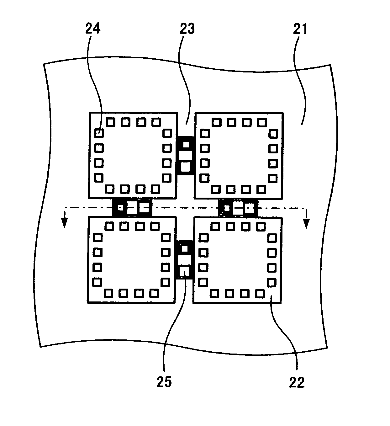
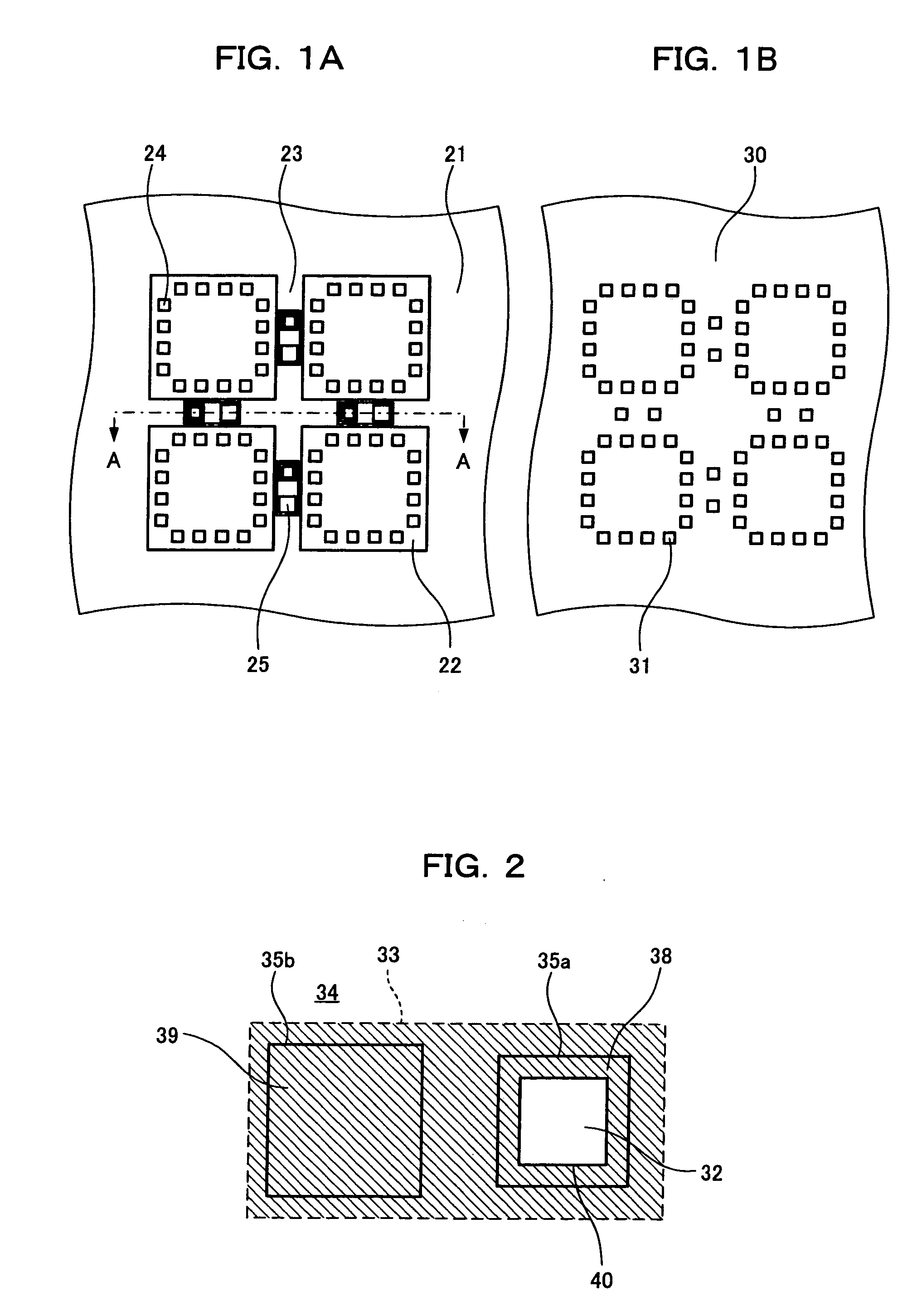
[0080]FIG. 1A is a plan view of a semiconductor wafer according to a first embodiment of the present invention; FIG. 1B is a plan view of a contactor for testing semiconductor devices on the wafer.

[0081] The semiconductor wafer 21 in FIG. 1A includes a number of semiconductor devices 22, scribe lines 23 for scribes formed between the semiconductors 22, and alignment patterns 25 formed inside the scribe lines 23. Electrode terminals 24 for connecting to the external are formed on each semiconductor device 22.

[0082] The alignment pattern 25 is used in a burn-in test or an electrical property test on the semiconductor wafer 21. In the first embodiment, more than one alignment pattern 25 is formed in each of the scribe lines 23 intersecting at right angles.

[0083] The contactor 30 in FIG. 1B is a testing tool for conducting burn-in tests or electrical property tests on the semiconductor wafer 21. The contactor 30 has on a substrate a number of bump electrodes 31 for testing some or al...

second embodiment

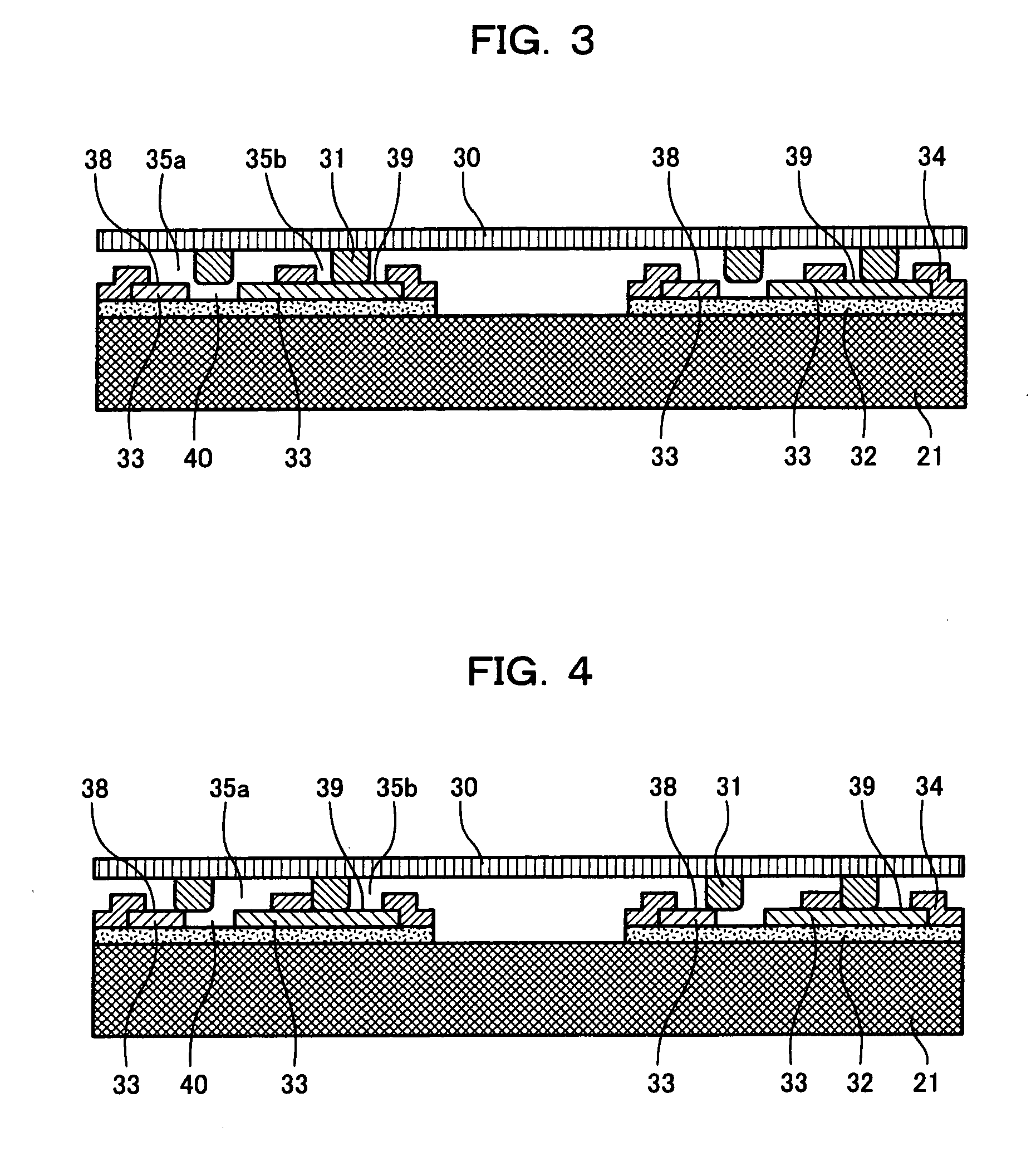
[0102] A second embodiment of the present invention will be described below. FIG. 6 is a plan view of an alignment pattern 25 and FIG. 7 is a cross-sectional view in direction of arrow B-B of FIG. 6.

[0103] The alignment pattern 25 in FIGS. 6 and 7 includes a rectangular conductor electrode terminal 39 formed by a conducting layer on an underlying insulating layer 32, and a detector electrode terminal 38 surrounding the conductor electrode terminal 39, except along one side of the conductor electrode terminal 39. A gap is provided between the conductor electrode terminal 39 and the detector electrode terminal 38. The gap may be filled with an insulator film such as SiN.

[0104] An upper insulating layer 34 formed over the underlying insulating layer 32 and the conducting layer 33 has a rectangular opening 35 above the detector electrode terminal 38 and the conductor electrode terminal 39. The entire conductor electrode terminal 39 is exposed in the opening 35 and the detector electro...

third embodiment

[0110] A third embodiment of the present invention will be described below. FIG. 9 is a plan view of an alignment pattern 25. The alignment pattern 25 in FIG. 9 includes a rectangular conductor electrode terminal 39 formed by a conducting layer on an underlying insulating layer 32, and a detector electrode terminal 38 opposed to and separated by a gap from one end of he conductor electrode terminal 39.

[0111] An upper insulating layer 34 provided over the underlying insulating layer 32 and the conducing layer 33 has an opening 35 above the detector electrode terminal 38 and the conductor electrode terminal 39. In the opening 35, a portion of the conductor electrode terminal 39 and a portion of the detector electrode terminal 38 are exposed from one of the sides of the perimeter of the opening 35, the portion of the detector electrode terminal 38 is exposed along one of the sides of the perimeter of the opening 35, and the underlying insulating layer 32 is exposed in the regions wher...


PUM


Abstract

Circuits under electrode terminals and a nonconductor layer of the electrode terminals in semiconductor devices are prevented from being damaged during a test, such as a burn-in test, on the semiconductor devices formed on a wafer. Alignment patterns provided on the semiconductor wafer have detector electrode terminals and conductor electrode terminals. A detector electrode terminal surrounds a conductor electrode terminal separated by a gap from the detector electrode terminals and a portion of the surrounding detector electrode terminal is open.

Description

FIELD OF THE INVENTION [0001] The present invention relates to a semiconductor wafer and a testing method therefore, and in particular to a semiconductor wafer having alignment patterns for conducting tests on the semiconductor wafer and a testing method conducting tests on the semiconductor wafer. BACKGROUND OF THE INVENTION [0002] Electrical property tests and potential defect burn-in screening tests of semiconductor devices on a wafer have been conducted with a probe card including many probes. A number of semiconductor devices are formed on the semiconductor wafer and alignment patterns used in conducting a test of the wafer are provided on the wafer. [0003]FIG. 25 shows an enlarged view of a portion of conventional semiconductor wafer. Shown in FIG. 25 is an alignment pattern provided for one semiconductor device. [0004] In FIG. 25, an ion probe test on the internal circuitry of the semiconductor device 2 formed on the semiconductor wafer 1 is conducted with a probe card includ...

Claims


Application Information

Patent Timeline
Patent Type & Authority Applications(United States)
IPC IPC(8): G01R31/26
CPCG01R31/2855G01R31/2884G01R31/2891H01L2224/06H01L2224/0603
Inventor TAKAHASHI, MASAONAKATA, YOSHIROUMIMURA, TADAAKISAKASHITA, TOSHIHIKOFUKUDA, TOSHIYUKI
Owner PANASONIC SEMICON SOLUTIONS CO LTD
Why Eureka
Try Eureka