Method in the fabrication of an integrated injection logic circuit

a logic circuit and injection logic technology, applied in the direction of basic electric elements, electrical equipment, semiconductor devices, etc., can solve the problems of not directly applicable to modern bipolar process technologies, increased fabrication cycle time, and high manufacturing cost, so as to increase the fabrication cycle time, process complexity, and process complexity.

Inactive Publication Date: 2006-05-18
INFINEON TECH AG
View PDF8 Cites 18 Cited by
  • Summary
  • Abstract
  • Description
  • Claims
  • Application Information

AI Technical Summary

Benefits of technology

[0012] The main drawback of BiCMOS technology is the high process complexity, which leads to higher fabrication costs and increased fabrication cycle time.
[0017] It would also be advantageous to provide such a method, which is simple and straight-forward and which requires a minimum of process steps.
[0019] It would also be advantageous to provide such a method, by which a compact and high density injection logic circuit can be fabricated.
[0020] Additionally, it would be advantageous to provide such a method, by which an injection logic circuit containing high performance transistors can be fabricated.
[0021] Yet another advantage would be to provide a method for manufacturing a radio transceiver device encompassing an integrated injection logic circuit and a bipolar amplifier device in bipolar process.
[0022] Furthermore, it would be advantageous to provide an integrated injection logic circuit, which can be fabricated by a method having the above advantages, and which contains high performance transistors.

Problems solved by technology

The main drawback of BiCMOS technology is the high process complexity, which leads to higher fabrication costs and increased fabrication cycle time.
Conventional semiconductor processes for I2L are compatible with old diffused bipolar processes; however the concept is not directly applicable to modern bipolar process technologies.
The device disclosed in U.S. Pat. No. 5,504,368 requires a complex and non-conventional fabrication process.
Further, the device seems not to use available space optimally.

Method used


Image

  • Method in the fabrication of an integrated injection logic circuit
  • Method in the fabrication of an integrated injection logic circuit
  • Method in the fabrication of an integrated injection logic circuit

Examples


Embodiment Construction

[0064] In order to give a thorough understanding of the present invention various embodiments will be described. It will be apparent to one skilled in the art that the invention may be practiced in other embodiments that depart from those explicitly disclosed. In other instances, detailed descriptions of methods well-known to one skilled in the art are omitted.

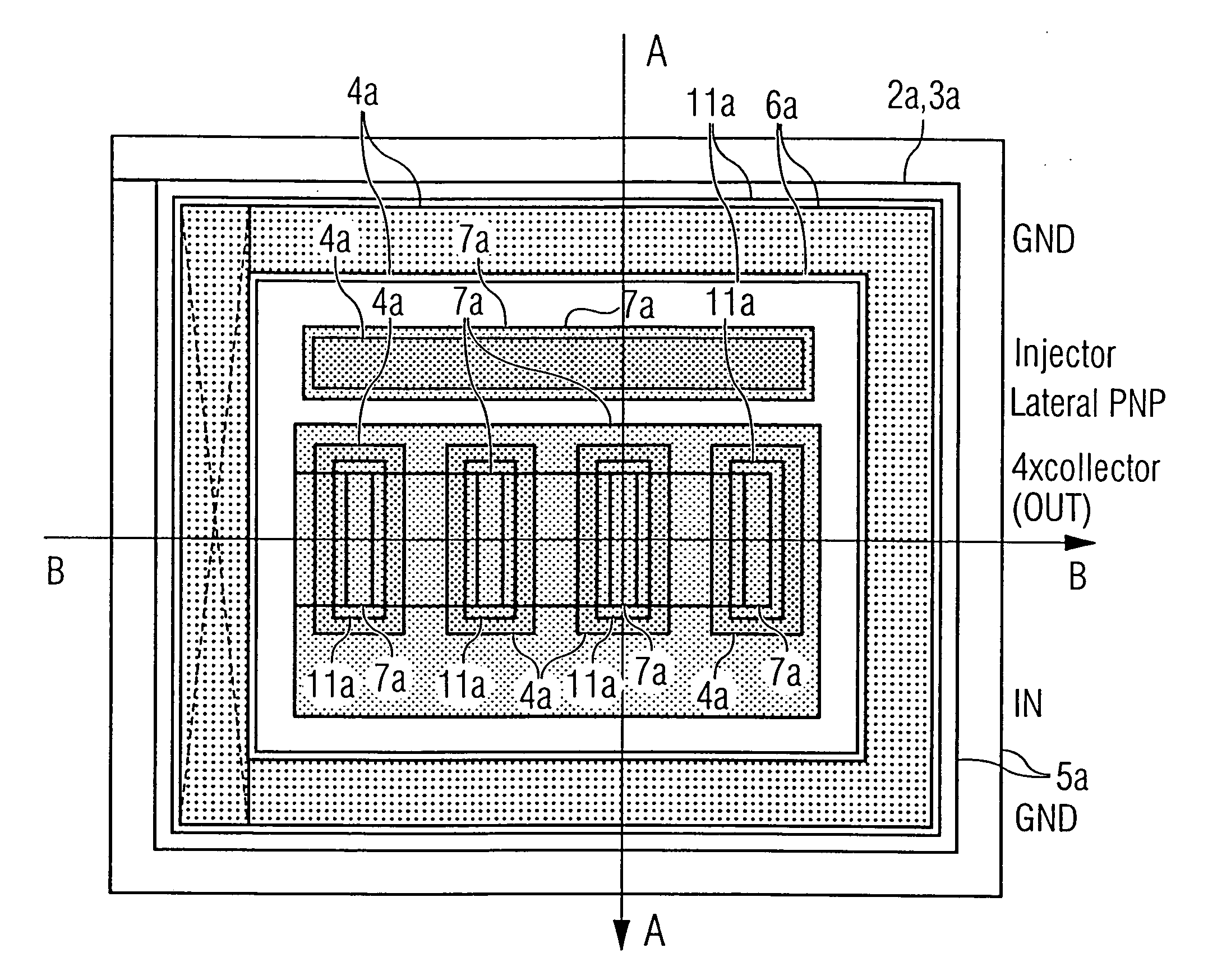
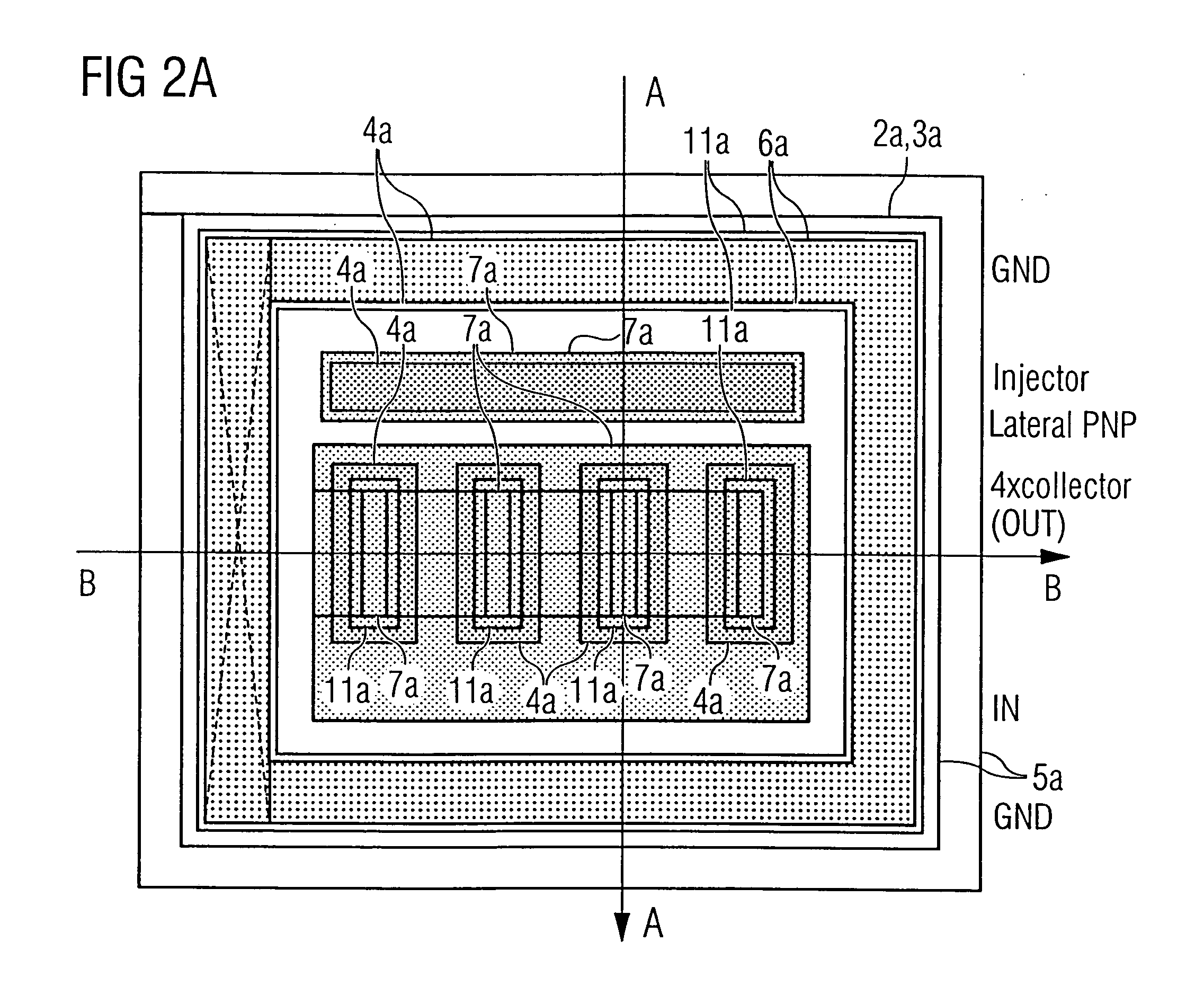
[0065] It shall be pointed out that the process steps described below are further detailed in the U.S. Pat. No. 6,610,578 and the international patent publication WO 02 / 091463 A1, the contents of which being hereby incorporated by reference. Particularly, the process steps described below may be performed simultaneously as corresponding process steps for fabrication of a high-performance bipolar transistor are performed. Such bipolar only process may be used for the fabrication of a radio transceiver device comprising amplifier structures and logic.

[0066] A first embodiment of a method in the fabrication of a monolithically ...


PUM


Abstract

A method in the fabrication of an I2L circuit comprises (i) forming a common base of a lateral bipolar transistor and emitter of a vertical bipolar multicollector transistor, a common collector of the lateral transistor and base of the vertical multicollector transistor, and an emitter of the lateral transistor in a substrate; (ii) forming, from a first deposited polycrystalline layer, a contact region for the common collector / base and a contact region for the emitter of the lateral transistor; (iii) forming an isolation structure for electric isolation of the polycrystalline contact region for the common collector / base; and (iv) forming, from a second deposited polycrystalline layer, a contact region for the common base / emitter and multiple collectors of the vertical multicollector transistor.

Description

CROSS-REFERENCE TO RELATED APPLICATION [0001] This application claims priority from European Patent Application No. 04023839.6, which was filed on Oct. 6, 2004 and is incorporated herein by reference in its entirety. BACKGROUND OF THE INVENTION [0002] 1. Field of the Invention [0003] The present invention generally relates to the field of integrated circuit technology, and more specifically the invention relates to a method in the fabrication of an integrated injection logic circuit, and to an integrated injection logic circuit. [0004] 2. Description of Prior Art [0005] BiCMOS technology combines bipolar and CMOS devices on a single chip. BiCMOS technology has proven to be very useful for the increased integration in circuits used for telecommunications, in particular wireless applications, since bipolar devices are widely utilized for high-frequency parts, e.g. for analog radio functions, while CMOS technology is used for digital and mixed signal parts, such as data interfaces with...

Claims


Application Information

Patent Timeline
Patent Type & Authority Applications(United States)
IPC IPC(8): H01L21/8238
CPCH01L21/8224H01L21/8226H01L27/0214H01L27/0237H01L27/0744H01L27/0821H01L29/6625H01L29/735
Inventor JOHANSSON, TEDNORSTROEM, HANS
Owner INFINEON TECH AG
Why Eureka
Try Eureka