
Method for designing semiconductor intgrated circuit and system for designing the same

a semiconductor integrated circuit and integrated circuit technology, applied in the field of semiconductor integrated circuit and system design of semiconductor integrated circuit, can solve problems such as failure to take into account the effect of fabrication factors, failure to conduct statistical circuit analysis, and failure to take into account circuit malfunctions

Inactive Publication Date: 2006-05-18
PANASONIC CORP
View PDF0 Cites 21 Cited by
  • Summary
  • Abstract
  • Description
  • Claims
  • Application Information

AI Technical Summary

Benefits of technology

[0020] It is therefore an object of the present invention to enable simulation of a variation of a clock skew equivalent to simulation of an entire clock tree to be efficiently performed in design of a semiconductor integrated circuit, i.e., to enable such simulation to be performed on a realistic circuit scale.
[0040] With the second system, the circuit simulation means allows a delay distribution to be calculated for each of divided clock circuit descriptions, so that analysis of each of the clock circuit descriptions is performed with the relationship among the divided clock circuit descriptions maintained. As a result, analysis equivalent to simulation of the entire clock circuit is performed within a realistic time by calculating a delay distribution for each of the divided clock circuit descriptions.

Problems solved by technology

A large skew causes a circuit malfunction.
However, in this reference, though a process of using clocks in the tree structure and calculating skews is disclosed, variations caused by fabrication factors are not taken into consideration and, in addition, no statistical circuit analysis is conducted.
Therefore, it is difficult to obtain a skew distribution with high accuracy, though the need for this is high.

Method used


Image

  • Method for designing semiconductor intgrated circuit and system for designing the same
  • Method for designing semiconductor intgrated circuit and system for designing the same
  • Method for designing semiconductor intgrated circuit and system for designing the same

Examples


embodiment 1

[0076] A system for designing a semiconductor integrated circuit according to a first embodiment of the present invention will be described with reference to the drawings. In the first embodiment, a circuit simulation system and a circuit simulation method using a variation in fabricating CMOS transistors, out of CMIS transistors, as a factor of variation in circuit characteristics will be described.

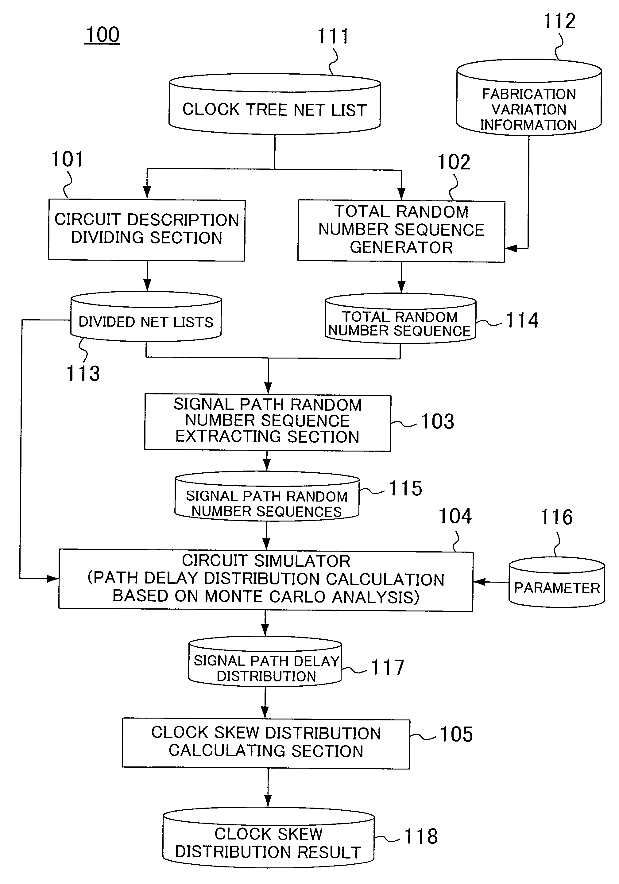
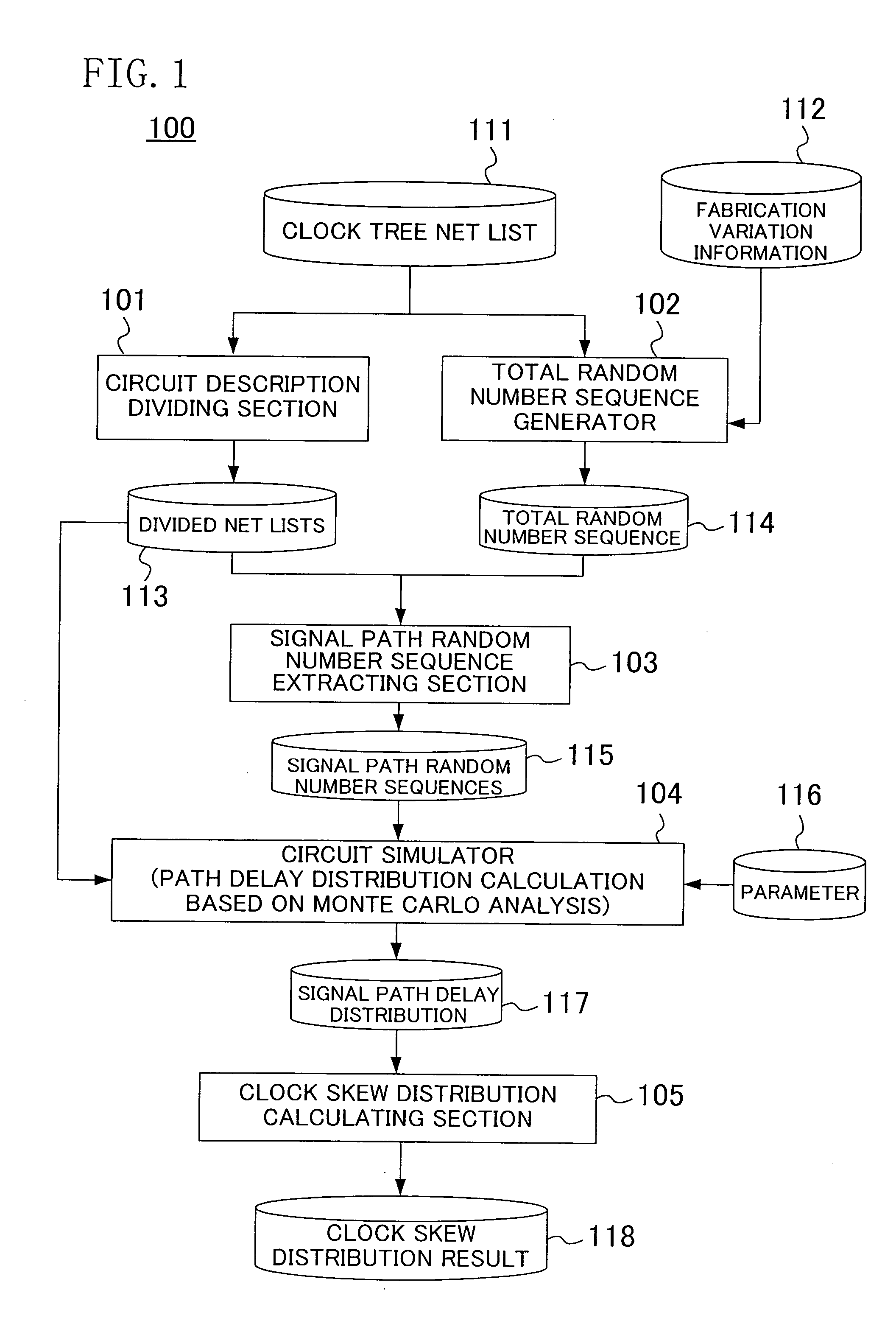
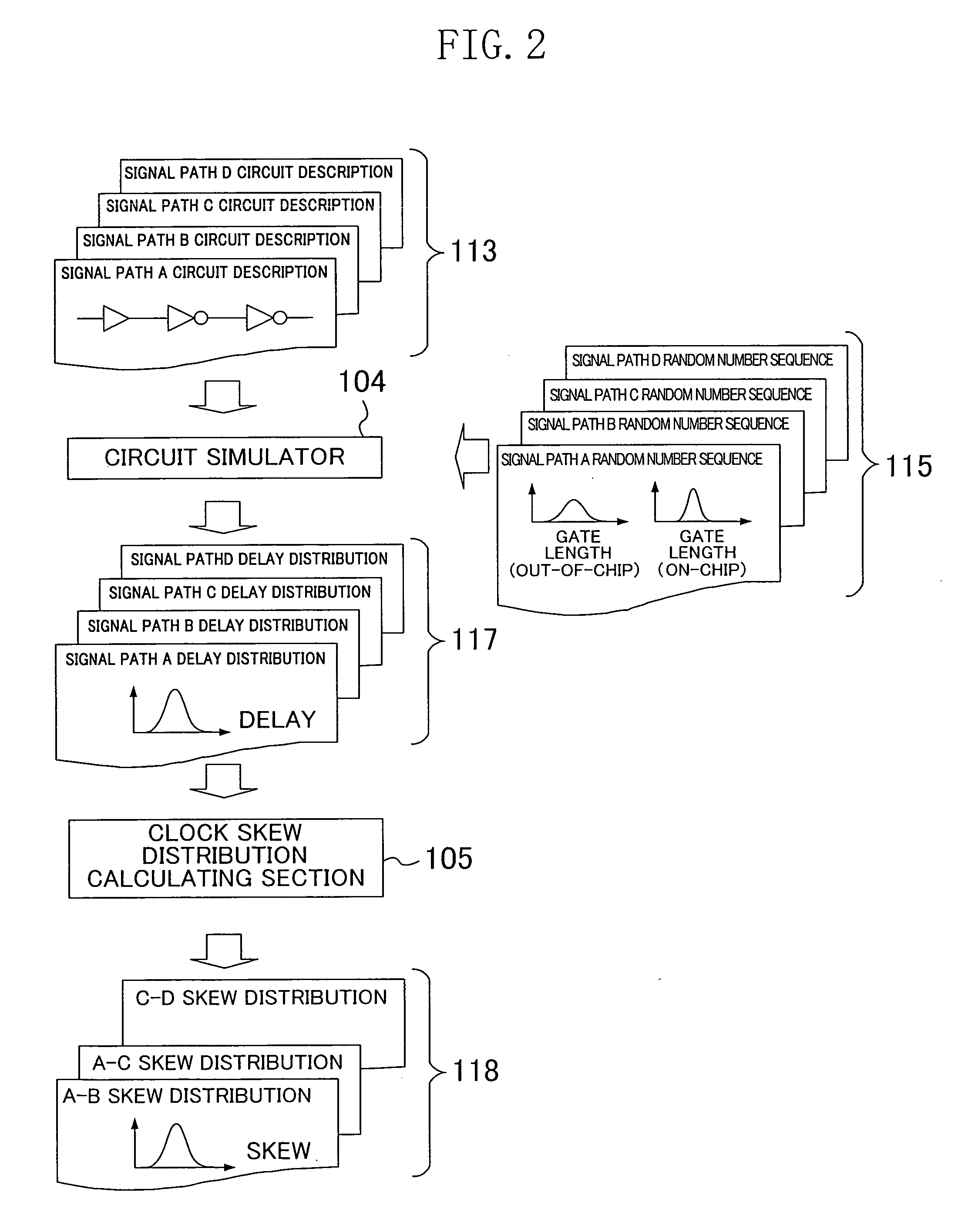
[0077]FIG. 1 is a block diagram of a circuit simulation system according to the first embodiment. As shown in FIG. 1, a circuit simulation system 100 according to the first embodiment includes: a circuit description dividing section 101; a total random number sequence generator 102; a signal path random number sequence extracting section 103; a circuit simulator 104; and a clock skew distribution calculating section 105.

[0078] The circuit description dividing section 101 reads a net list 111 that is a circuit description of a clock tree circuit on which circuit simulation as shown in F...

embodiment 2

[0131] Hereinafter, a system for designing a semiconductor integrated circuit and operation thereof according to a second embodiment of the present invention will be described with reference to the drawings. In this embodiment, fabrication variation in CMOS transistors is also exemplified.

[0132] The design system of the second embodiment has a configuration similar to that of the first embodiment illustrated in FIG. 1 and is different from that of the first embodiment in that the circuit description dividing section 101 does not divide a circuit to be designed in units of signal paths but divides the circuit in units of blocks each having a plurality of signal routes.

[0133] Now, operation of the system for designing a semiconductor integrated circuit of the second embodiment will be described. A total random number sequence generating step S1 is identical to that in the first embodiment, and description thereof is omitted.

(Circuit Description Dividing Step S2)

[0134] A circuit d...

embodiment 3

[0146] Hereinafter, a system for designing a semiconductor integrated circuit and operation thereof according to a third embodiment of the present invention will be described with reference to the drawings. In this embodiment, fabrication variation in CMOS transistors is also exemplified.

[0147] The design system of the third embodiment is similar to that of the first embodiment shown in FIG. 1 and is different in that a circuit description dividing section 101 divides a circuit including fan-out gates electrically connected to signal routes (signal paths) into signal path units.

[0148] In the third embodiment, as a clock tree circuit to be designed, a circuit including flip-flops FF1 through FF4 as illustrated in FIG. 18 is used. This is because output 10 terminals of a clock tree circuit are often connected to flip-flops in general.

[0149] As illustrated in FIG. 18, each of the flip-flops FF1 through FF4 includes a clock terminal C, a data terminal D, an output terminal Q and an i...


PUM


Abstract

A total random number sequence generator generates a total random number sequence of an entire circuit, as fabrication variation. A signal path random number sequence extracting section extracts, from the total random number sequence, a signal path random number sequence for a partial circuit obtained by dividing the entire circuit. A circuit simulating section executes Monte Carlo analysis using the signal path random number sequence for each partial circuit, thereby obtaining a desired circuit characteristic distribution. In this manner, correlation is maintained between divided circuit characteristic distributions and, in addition, the obtained circuit characteristic distribution is used for clock skew distribution calculation and others. Moreover, the circuit scale of a target of circuit simulation is reduced.

Description

CROSS-REFERENCE TO RELATED APPLICATION [0001] The disclosure of Japanese Patent Application No. 2004-332151 filed on Nov. 16, 2004 including specification, drawings and claims is incorporated herein by reference in its entirety. BACKGROUND OF THE INVENTION [0002] The present invention relates to methods for designing semiconductor integrated circuits and systems for designing semiconductor integrated circuits. In particular, the present invention relates to a method for designing a semiconductor integrated circuit that performs, in designing, for example, a system LSI (large scale integrated circuit), circuit simulation for evaluating variations in circuit characteristic, especially characteristics of a clock circuit, derived from variations in fabrication, and also relates to a system for designing the circuit. [0003] With recent development in fabrication techniques, the size of transistors has been reduced and the integration degree thereof has been rapidly increased. Accordingly...

Claims


Application Information

Patent Timeline
Patent Type & Authority Applications(United States)
IPC IPC(8): G06F17/50G06F9/45G06G7/62
CPCG06F17/5022G06F17/5045G06F30/30G06F30/33G06F30/3308G06F30/396
Inventor YONEZAWA, HIROKAZU
Owner PANASONIC CORP
Learn More