Laser cutting apparatus and laser cutting method

a laser cutting and laser cutting technology, applied in metal working equipment, welding/soldering/cutting articles, manufacturing tools, etc., can solve the problems of limited starting point for cutting, serious affecting the reliability of function elements, and limited logic circuits

Inactive Publication Date: 2006-05-25
CANON KK
View PDF10 Cites 56 Cited by
  • Summary
  • Abstract
  • Description
  • Claims
  • Application Information

AI Technical Summary

Benefits of technology

[0013] In one aspect of at least one exemplary embodiment, a laser cutting method, which is adapted to concentrate laser light to a light concentrating point at a predetermined depth inside a material from a surface of the material to form an internal processing region and adapted to cut the material to separate the surface of the material into a plurality of regions, includes a step of changing, when an irradiation pulse train is generated by concentrating a plurality of laser beams to the light concentrating point, a composite duration of the irradiation pulse train, and a step of forming the internal processing region by irradiating the material with the generated irradiation pulse train.
[0014] In another aspect of at least one exemplary embodiment, a laser cutting method and a laser cutting apparatus, which are adapted to concentrate laser light to a light concentrating point at a predetermined depth inside a material from a surface of the material to form an internal processing region and adapted to cut the material to separate the surface of the material into a plurality of regions, are configured to generate an irradiation pulse train by concentrating a plurality of laser beams to the light concentrating point, and to change a size of the internal processing region by changing a composite duration of the irradiation pulse train.

Problems solved by technology

Thus, there is a fear that the dusts seriously affect the reliability of the function elements.
However, this method has drawbacks in that parts of the surface of the substrate, which surround a cut part, are thermally melted, that especially, in the case where the substrate is a semiconductor substrate, logic circuits provided on the substrate are damaged, and that similarly to the blade dicing, problems due to dusts occur, because laser processing proceeds while melting the substrate from a laser light incidence side to a laser light exit side, so that dusts produced by resolidification of melted materials adhere to the surface of the substrate.
However, a starting point for cutting is limited by the aforementioned method to an internal processing region inside a material to be cut.
Thus, it is difficult to precisely control the direction and the position of a crack that reaches the surface of the material from the starting point.
In a case where the length in the direction of depth of the internal processing region formed in the material to be cut is too long and, thus, a crack reaches the surface of the material, the crack appearing in the surface of the material causes a spurt of dust.
Additionally, in a case where a functional device is formed on the surface of the material, the functional device is damaged.
Especially, in a case where the material to be cut is a silicon wafer, the development of the crack is easily affected by a crystal orientation.
Therefore, in a case where there is a misalignment between a predetermined cutting line and the crystal orientation due to an industrial error caused when a silicon substrate and devices are formed, according to the aforementioned laser processing method, a crack deviating from the predetermined cutting line in the process of developing in the surface may break down logic circuits provided in device portions.
Thus, a problem arises in that a crack extends to such a structure, so that the substrate is broken down.
This problem often arises in a case where the thickness of the substrate is large relative to a modified layer formed inside the substrate.

Method used


Image

  • Laser cutting apparatus and laser cutting method
  • Laser cutting apparatus and laser cutting method
  • Laser cutting apparatus and laser cutting method

Examples


Embodiment Construction

[0032] Exemplary embodiments of the invention will be described in detail below with reference to the drawings. However, the dimensions, materials, shapes and relative positions of the constituent parts shown in the embodiments should be changed as convenient depending on various conditions and on the structure of the apparatus adapted to the invention, and the invention is not limited to the embodiments described herein.

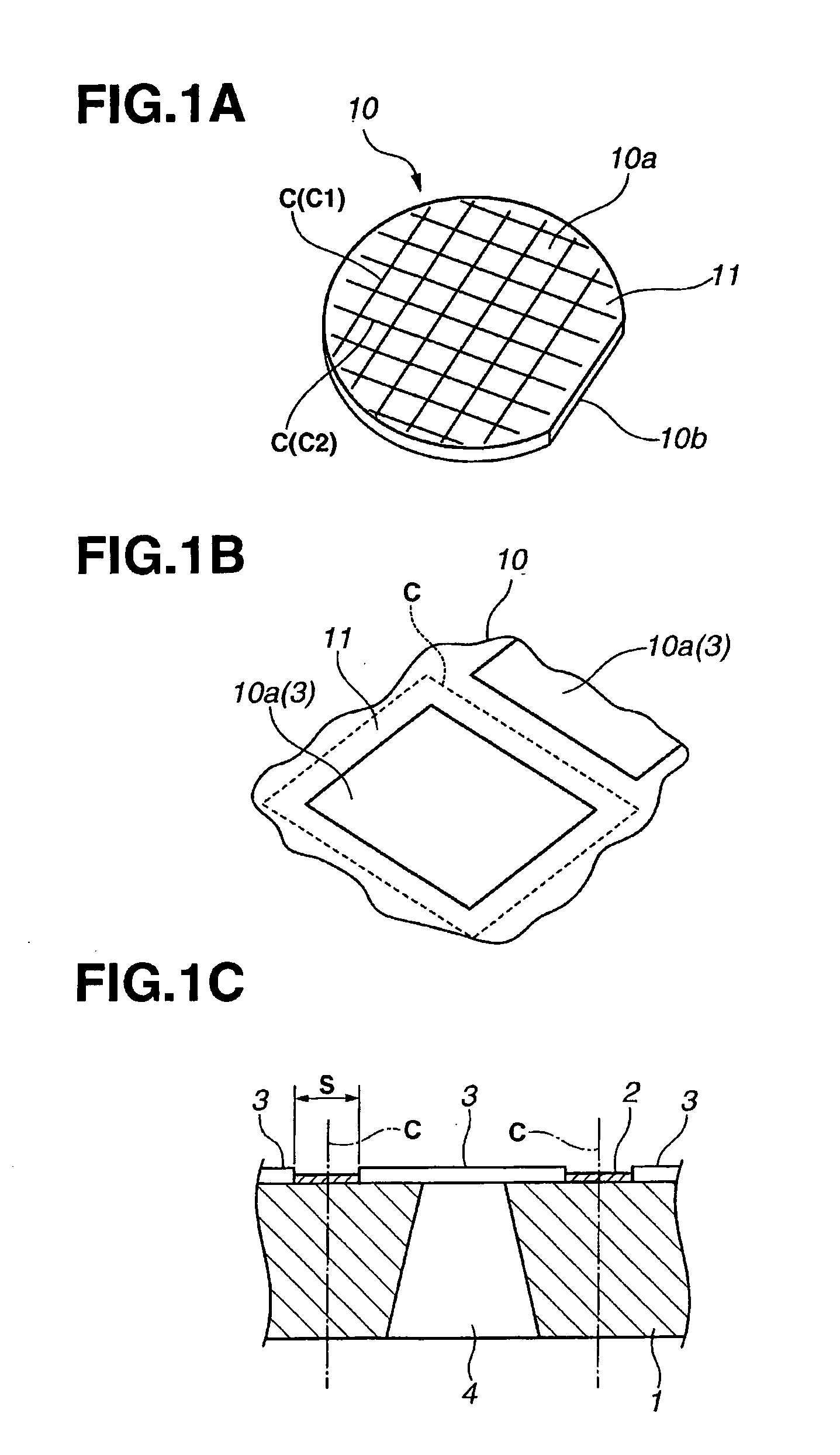
[0033] Description of the embodiments is started by explaining a cutting method of using a silicon substrate 10, on the surface of which a plurality of logic element portions 10a serving as semiconductor device portions are formed as shown in FIG. 1A, as an example of a material to be cut, and separating the silicon substrate 10 into the logic element portions 10a as device chips.

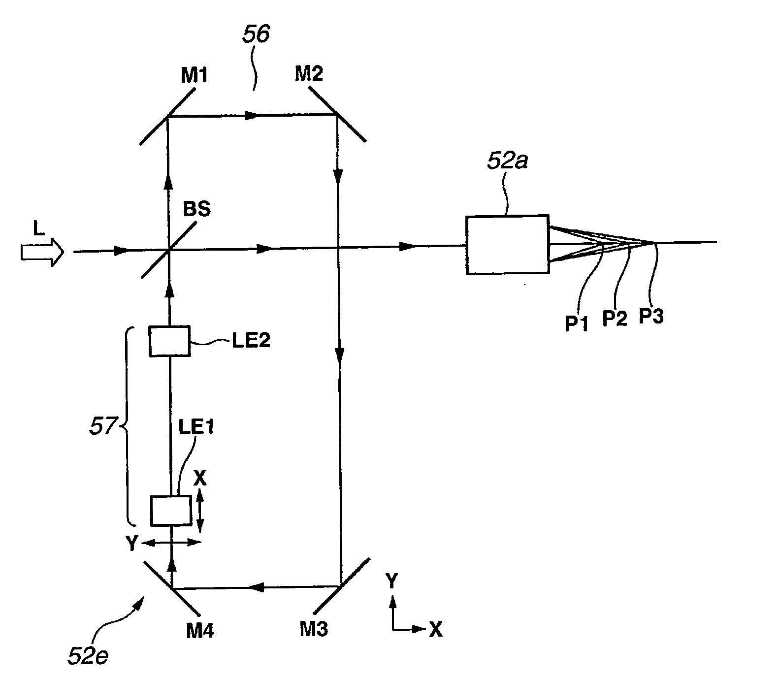
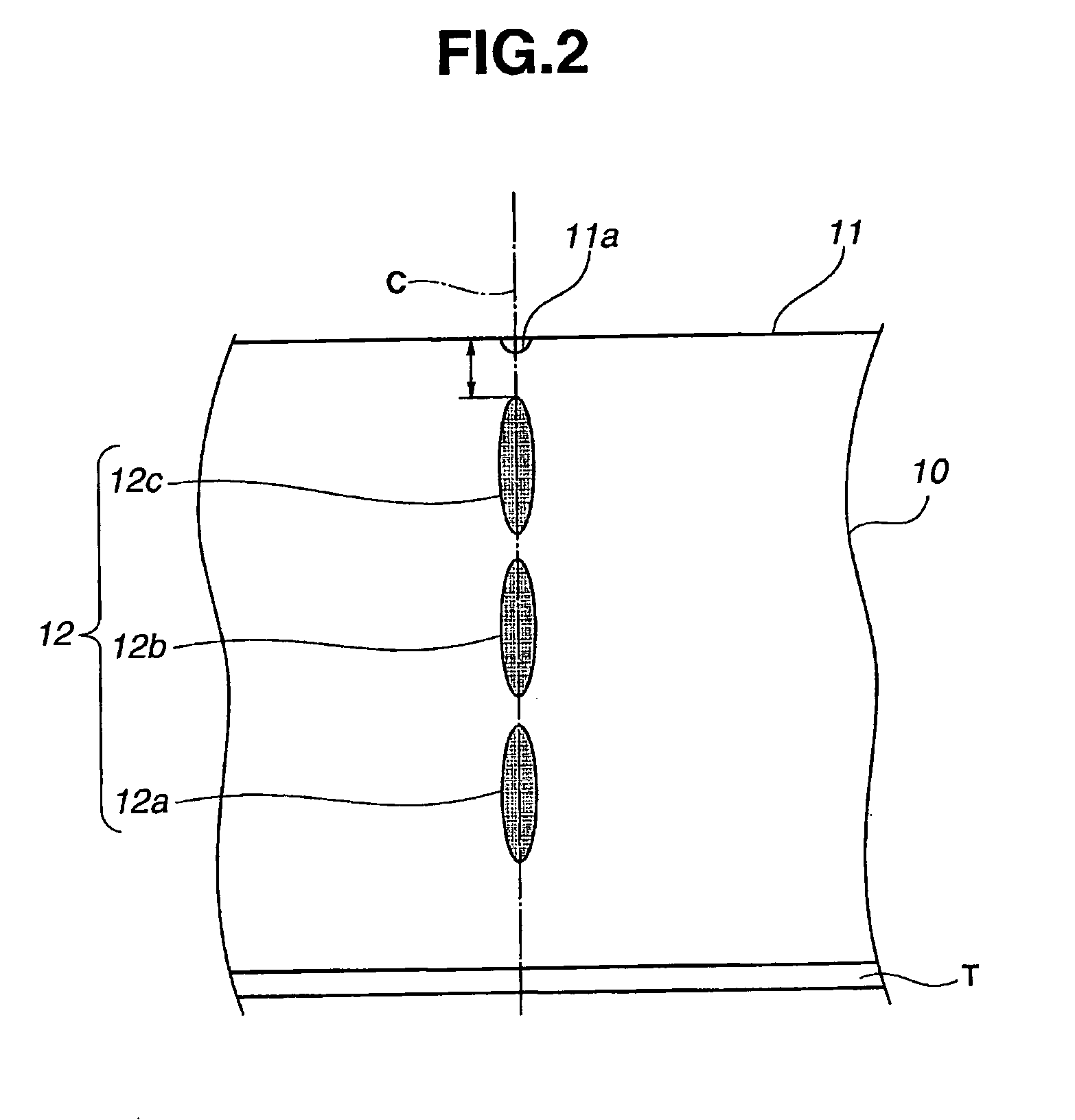
[0034] As shown in FIG. 2, laser light is concentrated to a light concentrating point at a predetermined depth inside the substrate from a surface 11 thereof to thereby form an internal p...


PUM

PropertyMeasurementUnit
thicknessaaaaaaaaaa
thicknessaaaaaaaaaa
depthaaaaaaaaaa

Abstract

A laser cutting apparatus and a laser cutting method are provided which are adapted to concentrate laser light into a silicon substrate to produce a plurality of internal cracks. A light concentrating position, to which laser beams included in the laser light are concentrated, is temporally and spatially displaced to appropriately change lengths of the cracks according to positions in a direction of depth of the substrate. Consequently, the lengths of the internal cracks are controlled to surely lead a crack opening, the starting point of which is the internal crack formed by laser processing, to a predetermined cutting line on a surface of the substrate.

Description

BACKGROUND OF THE INVENTION [0001] 1. Field of the Invention [0002] The present invention relates to a laser cutting apparatus and a laser cutting method which are adapted to cut a material by concentrating laser light into the material to separate the material into a plurality of regions. [0003] 2. Description of the Related Art [0004] Hitherto, there are various techniques of separating a surface of a material, which is to be cut, into a plurality of areas by concentrating laser light into the material to thereby cut the material. An example of the techniques is a known blade dicing method adapted to rotate a circular blade, which has a width ranging from tens μm to hundreds μm, at a high speed in a case where a semiconductor substrate, such as a silicon wafer, is precisely cut into semiconductor chips, so that the substrate is abraded by abrasives provided on the surface of the blade to cut the substrate. According to this method, coolant water is sprayed onto a cutting surface s...

Claims


Application Information

Patent Timeline
Patent Type & Authority Applications(United States)
IPC IPC(8): B23K26/38B23K26/06
CPCB23K26/063B23K26/38B23K26/407B23K26/0676B23K2201/40B23K26/0057B23K26/0617B23K26/4075B23K26/0622B23K26/40B23K26/53B23K2101/40B23K2103/50
Inventor NISHIWAKI, MASAYUKIIRI, JUNICHIROINADA, GENJISUGAMA, SADAYUKI
Owner CANON KK
Why Eureka
Try Eureka