Photoactive devices and components with enhanced efficiency

Inactive Publication Date: 2006-06-01
NANOSYS INC
View PDF45 Cites 84 Cited by
  • Summary
  • Abstract
  • Description
  • Claims
  • Application Information

AI Technical Summary

Benefits of technology

[0008] The present invention is directed to improved photoactive devices and components that make up such devices. In particular, the invention relates to improved compositions, architectures and processes whereby one can produce photoactive devices that more ef

Problems solved by technology

In photoactive devices, the losses at each of these steps substantially affect the overall efficiency of the device.
It is the inefficiencies at these steps that can have some of the most substantial impacts on the conversions efficiency, and for example, are among the major stumbling blocks of cost effective solar energy, as the costs associated with producing more efficient devices, and their resulting yields, have not yet moved into the realm of cost effectiveness relat

Method used


Image

  • Photoactive devices and components with enhanced efficiency
  • Photoactive devices and components with enhanced efficiency
  • Photoactive devices and components with enhanced efficiency

Examples


Embodiment Construction

I. GENERAL OPERATION OF NANOCOMPOSITE PHOTOACTIVE SYSTEMS

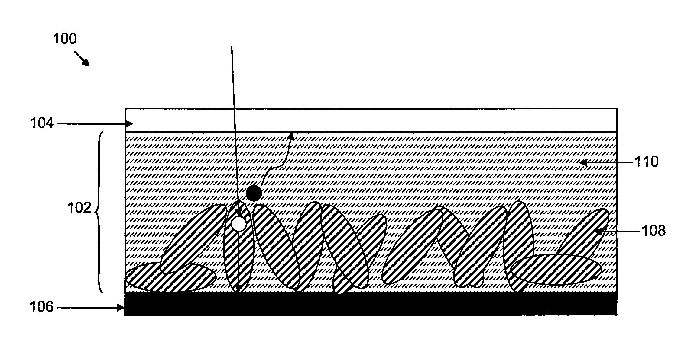
[0026] Nanocomposite photoactive or photovoltaic devices have been previously described in the art. For example, Published U.S. Patent Application No. 20040118448 (incorporated herein by reference in its entirety for all purposes) describes photovoltaic devices that employ a nanocomposite active layer sandwiched between two electrode layers. The active layer includes semiconductor nanocrystals dispersed within a conductive polymer matrix. Together, the nanocrystals and polymer form a diode, where the nanocrystal and polymer posses a type-II energy band gap offset relative to each other. When the nanocrystals are exposed to light, an electron is displaced from its orbital within the nanocrystal, giving rise to an electron-hole pair, collectively referred to as an “exciton” within the nanocrystal. Typically, when the exciton is allowed to recombine within the nanocrystal, it results in a release of the stored energy, e.g., in th...


PUM

PropertyMeasurementUnit
Thicknessaaaaaaaaaa
Angleaaaaaaaaaa
Lengthaaaaaaaaaa

Abstract

Devices, compositions and methods for producing photoactive devices, systems and compositions that have improved conversion efficiencies relative to previously described devices, systems and compositions. This improved efficiency is generally obtained by one or both of improving the efficiency of light absorption into the photoactive component, and improving the efficiency of energy extraction from that active component.

Description

CROSS-REFERENCE TO RELATED APPLICATIONS [0001] This application claims priority to U.S. Provisional Patent Application No. 60 / 629,095, filed Nov. 17, 2004, which is incorporated in its entirety herein.STATEMENT REGARDING FEDERALLY SPONSORED RESEARCH [0002] Portions of this invention may have been made with United States Government support under National Reconnaissance Office Prime Contract No. NRO-000-01-C-0130. As such, the United States Government may have certain rights in the invention.BACKGROUND OF THE INVENTION [0003] For photoactive devices and systems, the utility of the device or system is generally measured in terms of the efficiency with which it takes the ambient or incident light and converts that light to another form of energy, e.g., electricity, heat or light of different wavelength. The overall conversion efficiency is impacted by a number of factors for any given circumstance, including the amount of ambient light that impacts the photoactive components of the devi...

Claims


Application Information

Patent Timeline
IPC IPC(8): H01L21/00
CPCH01L27/302H01L31/0384H01L51/0007H01L51/0036H01L51/0037H01L51/4213H01L31/056H01L51/4253H01L51/426H01L51/447Y02E10/52Y02E10/549H01L51/424Y02P70/50H10K30/57H10K71/15H10K85/1135H10K85/113H10K30/10H10K30/20H10K30/35H10K30/87H10K30/30
Inventor PARCE, J. WALLACECHOW, CALVIN Y.H.MEISEL, ANDREAS P.NGUYEN, LINHSCHER, ERIK C.WHITEFORD, JEFFERY A.
Owner NANOSYS INC
Why Eureka
Try Eureka