Supercharge Your Innovation With Domain-Expert AI Agents!

Start signal outputting circuit

a signal and circuit technology, applied in the direction of pulse manipulation, amplitude demodulation, pulse technique, etc., can solve the problems of high frequency power leakage to the substrate, long resistance element, large space,

Active Publication Date: 2006-06-01
DENSO CORP
View PDF18 Cites 0 Cited by
  • Summary
  • Abstract
  • Description
  • Claims
  • Application Information

AI Technical Summary

Benefits of technology

[0015] Other characteristics and excellent effects of the invention will become clear from the following description of embodiments using drawings.

Problems solved by technology

When a resistance having a large resistance value like this is realized on an IC chip, the resistance element becomes long, and a large space becomes necessary.
As a result, the facing area of the resistance element facing ground becomes large, a parasitic capacitance and a parasitic resistance arise between the resistance on the chip and the ground in the substrate, and the high frequency power leaks to the substrate.
Consequently, to convert a low-level high frequency power of for example 5.8 GHz, −60 dBm into a direct current with a diode circuit formed on an IC chip is difficult.
Although it is possible to convert a low-level high frequency wave of −60 dBm into a direct current by using heterodyne detection technology, a transmitter or LAN and mixer must be operated continually, and the power consumed during high frequency signal standby time becomes large.
Also, with a high frequency detection circuit using a diode, it is notable that when the load resistance is large, the voltage applied across the anode / cathode of the diode becomes small and the high frequency wave cannot be converted, and that post-conversion output resulting from bias fluctuation is not distinguishable from d.c. potential obtained by converting high frequency power.

Method used


Image

  • Start signal outputting circuit
  • Start signal outputting circuit
  • Start signal outputting circuit

Examples


first embodiment

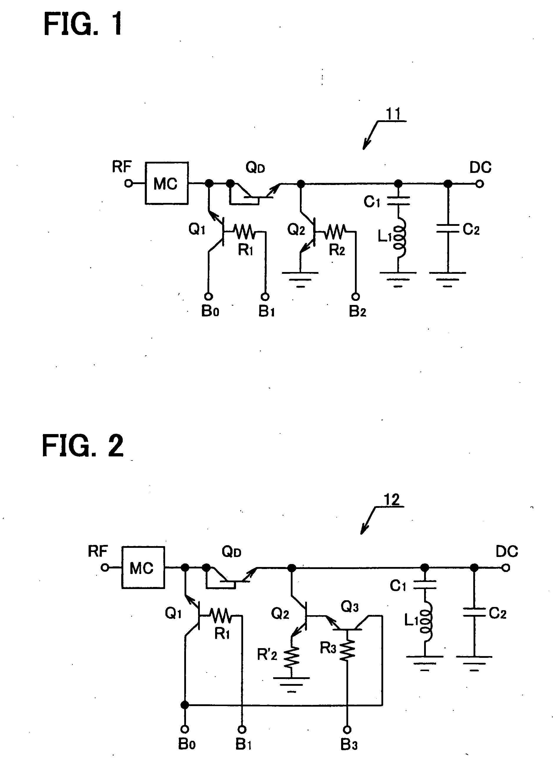
[0019]FIG. 1 is a circuit diagram showing an RF / DC-conversion circuit 11 constituting a main part of a start signal outputting circuit according to a first embodiment of the invention. The RF / DC-conversion circuit 11 is made up of a matching circuit MC; an npn transistor QD used as a diode; an npn transistor Q1 having its emitter connected to the base (anode side) of the npn transistor QD; a resistance R1 connected to the base of the npn transistor Q1; an npn transistor Q2 having its collector connected to the emitter (cathode side) of the npn transistor QD; a resistance R2 connected to the base of the npn transistor Q2; a capacitance C1 and an inductance L1 connected in series with the emitter (cathode side) of the npn transistor QD; and a capacitance C2 also connected to the emitter (cathode side) of the npn transistor QD.

[0020] A potential B0 is applied to the collector of the npn transistor Q1 and a potential B1 to the base via the resistance R1. The npn transistor Q2 has its e...

second embodiment

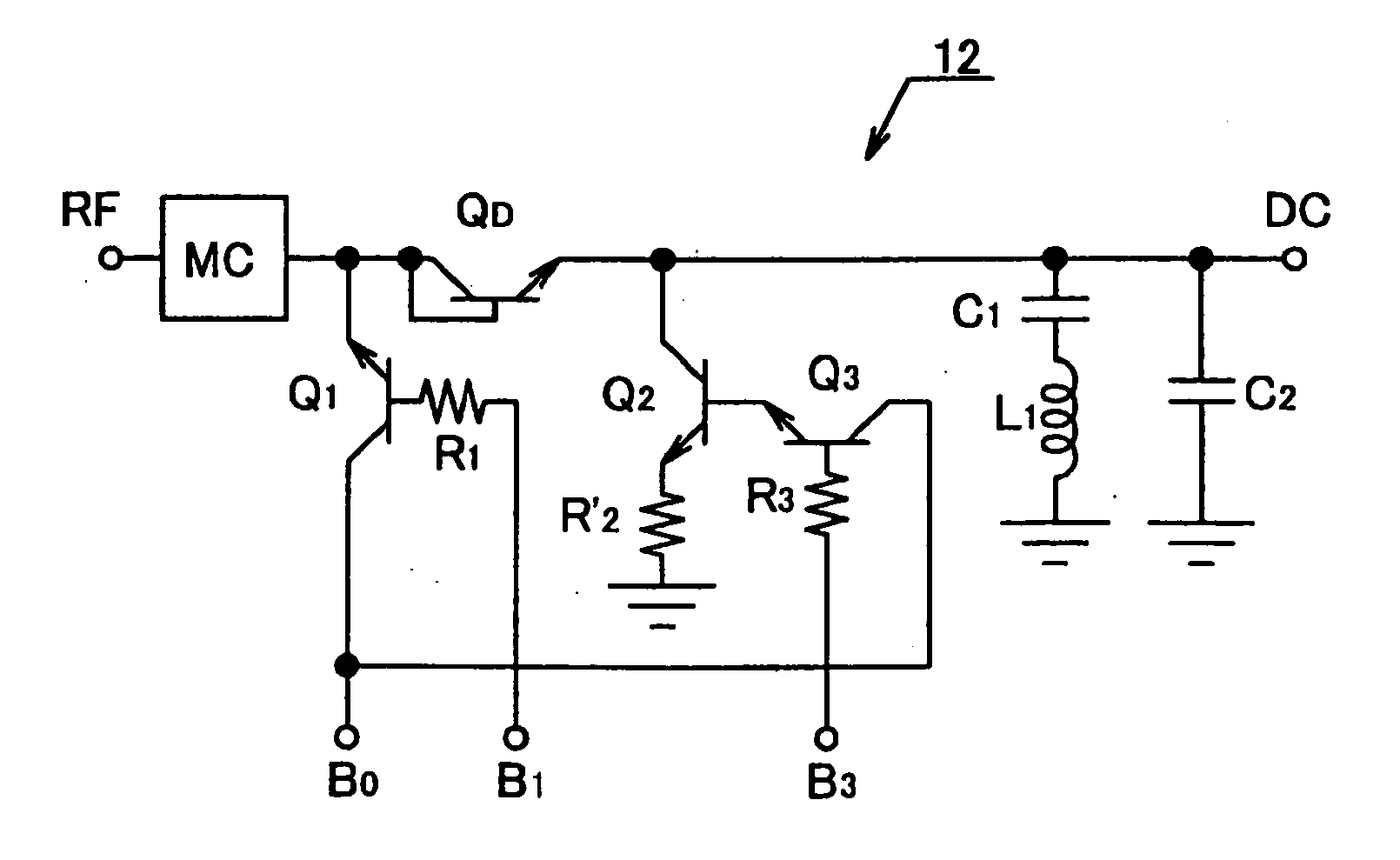
[0026]FIG. 2 is a circuit diagram showing an RF / DC-conversion circuit 12 constituting a main part of a start signal outputting circuit according to a second embodiment of the invention. From the construction of the RF / DC-conversion circuit 11 of FIG. 1, the RF / DC-conversion circuit 12 has the resistance R2 connected to the base of the npn transistor Q2 removed along with the bias potential B2. In their place, a resistance R′2 is provided between the emitter of the npn transistor Q2 and ground and the emitter of an npn transistor Q3 is connected to the base of the npn transistor Q2. A bias potential B3 is applied to the base of the npn transistor Q3via a resistance R3, and the bias potential B0 is applied to the collector of the npn transistor Q3.

[0027] The RF / DC-conversion circuit 12 of FIG. 2 was made in view of the fact that it is difficult to freely adjust the potential of the cathode side (emitter) of the npn transistor QD which works as the diode of the RF / DC-conversion circui...

third embodiment

[0030] As a third embodiment of the invention, an RF / DC-conversion circuit 150 obtained by making the RF / DC-conversion circuit 12 of FIG. 2 a differential type is shown in FIG. 4. The RF / DC-conversion circuit 150 is made up of a matching circuit 110, a differential RF / DC convertor part 100, and a filter part 120. A high frequency signal is inputted to the differential RF / DC convertor part 100 through the matching circuit 110. The differential RF / DC convertor part 100 has substantially the same construction as the four transistors of the RF / DC-conversion circuit 12 of FIG. 2 in duplicate, and has two d.c. outputs. The filter part 120 performs low-pass filtering on each of the two d.c. outputs of the differential RF / DC convertor part 100. Of the differential RF / DC convertor part 100 of the RF / DC-conversion circuit 150 of FIG. 4, the construction which converts a high frequency wave to a d.c. potential is made up of npn transistors QRD, QR1, QR2, QR3 and resistances RR1, RR2, RR3, whic...


PUM


Abstract

A start signal outputting circuit according to the invention has a differential RF / DC convertor part 100 for converting a high frequency power (RF) into a d.c. potential (DC). The RF / DC convertor part 100 is formed by two transistors QRD,QDD working as a diode, and transistors QR1˜R3,QD1˜D3 and resistances RR1˜R3 for forming high resistances at anode sides andcathodesidesofthesediodes, respectively. Adifferential amplification part 200 disposed at a later stage of the diode has not only amplifying effect but also low-pass filtering effect together with filtering pars 120, 210 of its previous and later stages. In this case, it is designed so that current flowing through the respective circuits is about 2˜3 μA. As a result, even if the high frequency power of the specified frequency is weak, for example −60˜−40 dBm, a start signal outputting circuit 1000 which outputs a d.c. potential of 0.3˜2.4V, is suitable for integration and has a low power consumption can be obtained.

Description

TECHNICAL FIELD [0001] This invention relates to a novel start signal outputting circuit. Here a start signal outputting circuit is defined as a circuit for outputting a direct current potential (DC) when inputting a high frequency power (RF) of a certain frequency band. This definition naturally includes circuits which, when inputting a high frequency power (RF) in the respective band intermittently at short intervals, output a direct current potential (DC) intermittently in correspondence with this. An example of a related field of the invention is technology relating to diode wave detection and rectenna. BACKGROUND ART [0002] As technology relating to diode wave detection and rectenna, technologies disclosed in Japanese Patent No.2561023 (Document 1), Japanese Patent No. 2605827 (Document 2), JP-A-4-291167 (Document 3), JP-A-9-162644 (Document 4), Japanese Patent No. 2533800 (Document 5), and JP-B-6-48895 (Document 6) are known. Of these, Documents 1 through 4 disclose technology...

Claims


Application Information

Patent Timeline
IPC IPC(8): H03D3/00H03D1/00H03D1/10H03D1/18H03G1/00H03G3/30
CPCH03D1/18H03G1/0023H03G3/30
Inventor MIZUNO, KAZUOKIMURA, RYUUDA, HISANORIHAYASHI, HIROAKI
Owner DENSO CORP
Features
  • R&D
  • Intellectual Property
  • Life Sciences
  • Materials
  • Tech Scout
  • Unparalleled Data Quality
  • Higher Quality Content
  • 60% Fewer Hallucinations
Learn More