Magnetic random access memory
- Summary
- Abstract
- Description
- Claims
- Application Information
AI Technical Summary
Benefits of technology
Problems solved by technology
Method used
Image

Examples
first embodiment
(1) First Embodiment
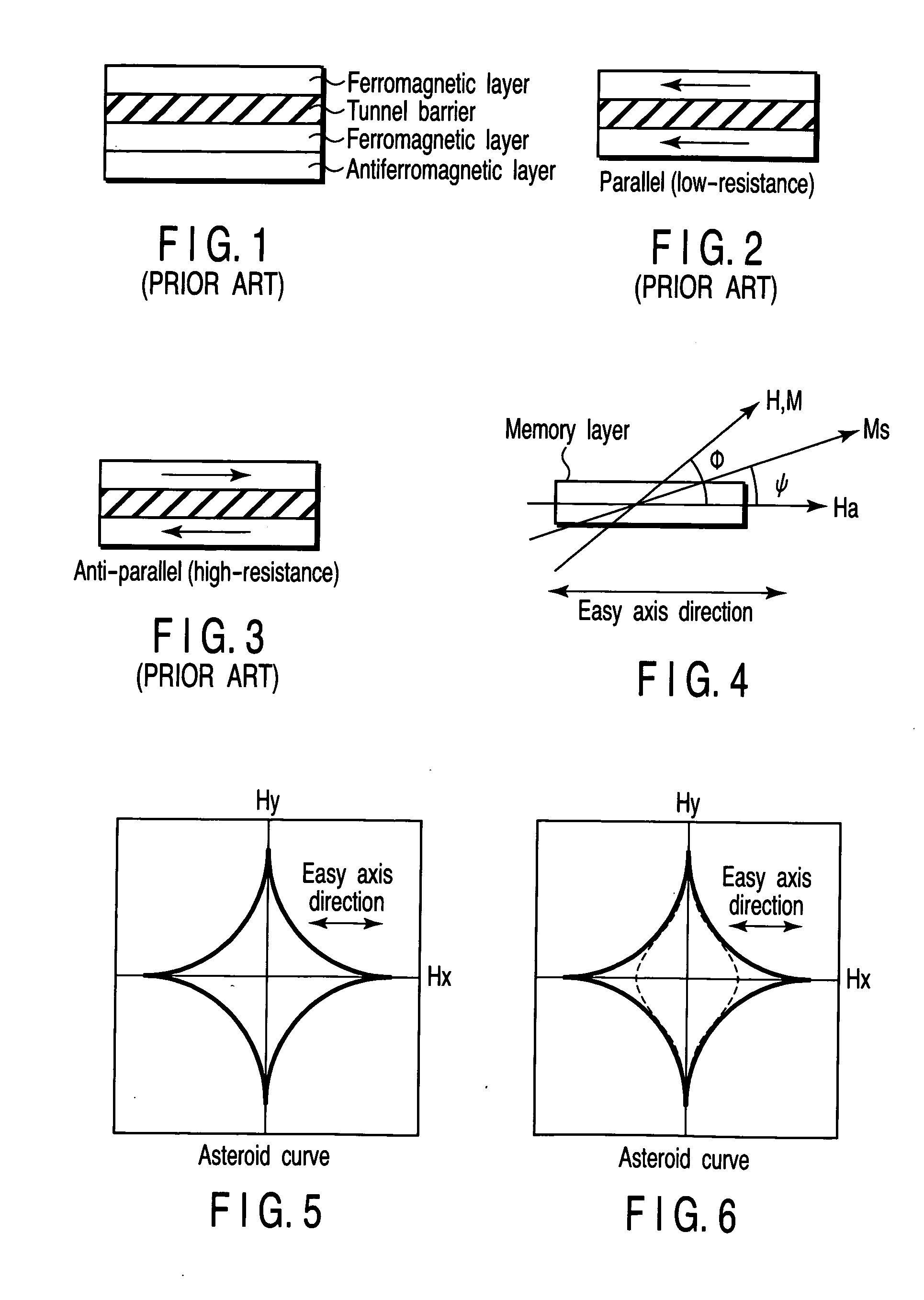
[0119] A first embodiment of the invention relates to a technique in which a switching magnetic field of a half-selected MTJ element is selectively made great by applying a stress to the half-selected MTJ element at the time of data writing.
A. Memory Cell
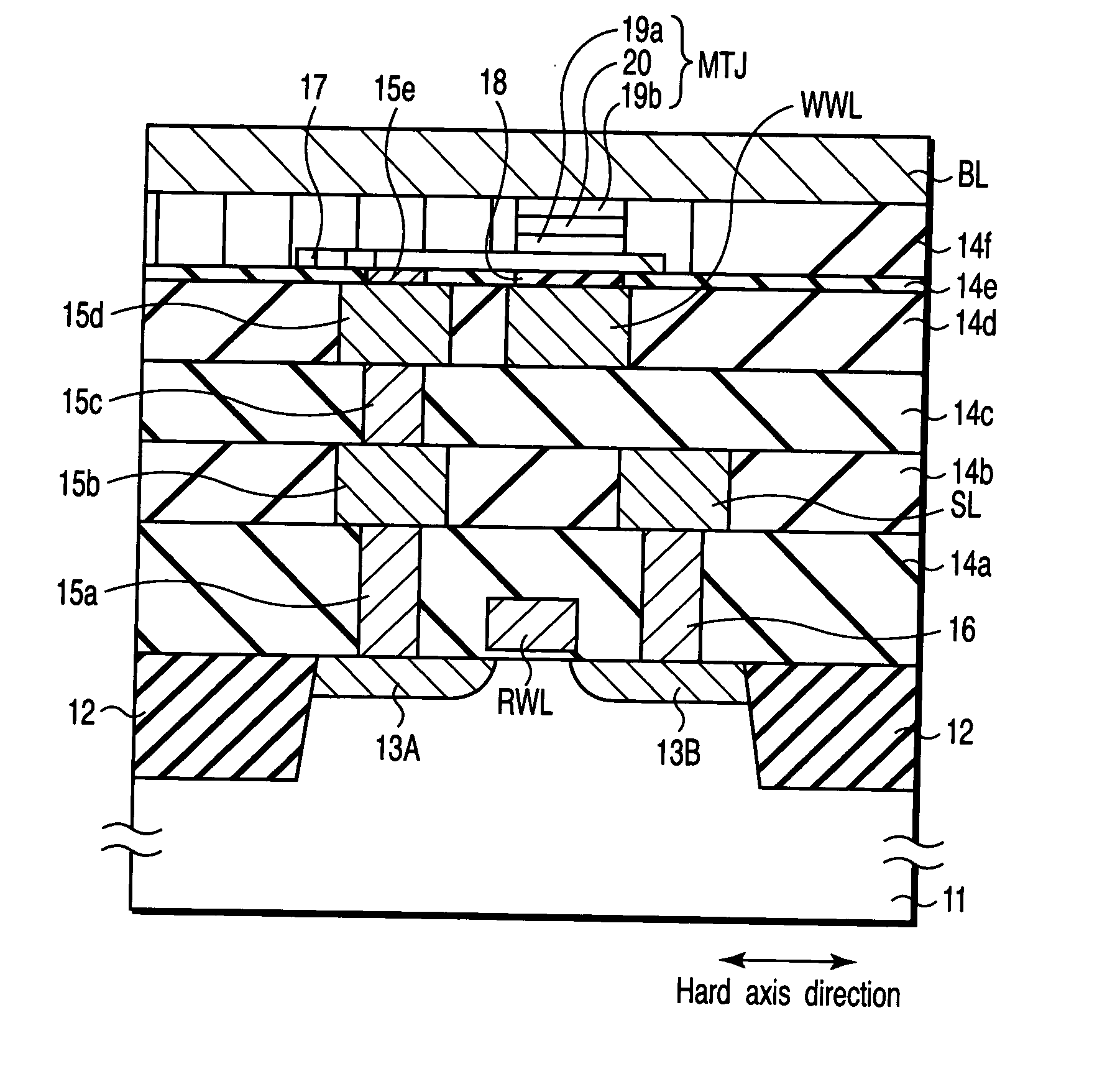
[0120]FIG. 12 shows a structure of a memory cell of a magnetic random access memory according to the first embodiment.
[0121] In the present embodiment, a 1MOST+1MTJ type memory cell formed from one transistor and one MTJ element is an object.
[0122] Element isolation regions 12 having the STI (Shallow Trench Isolation) structure are formed on a surface region of a semiconductor substrate 11. A MOS transistor serving as a read selective switch is formed within an element region surrounded by the element isolation regions 12. The gate of the MOS transistor will be served as a read word line RWL.
[0123] A drain 13A of the MOS transistor is connected to a lower metal layer 17 via contact plugs 15a, 15c, and 15e, ...
second embodiment
(2) Second Embodiment
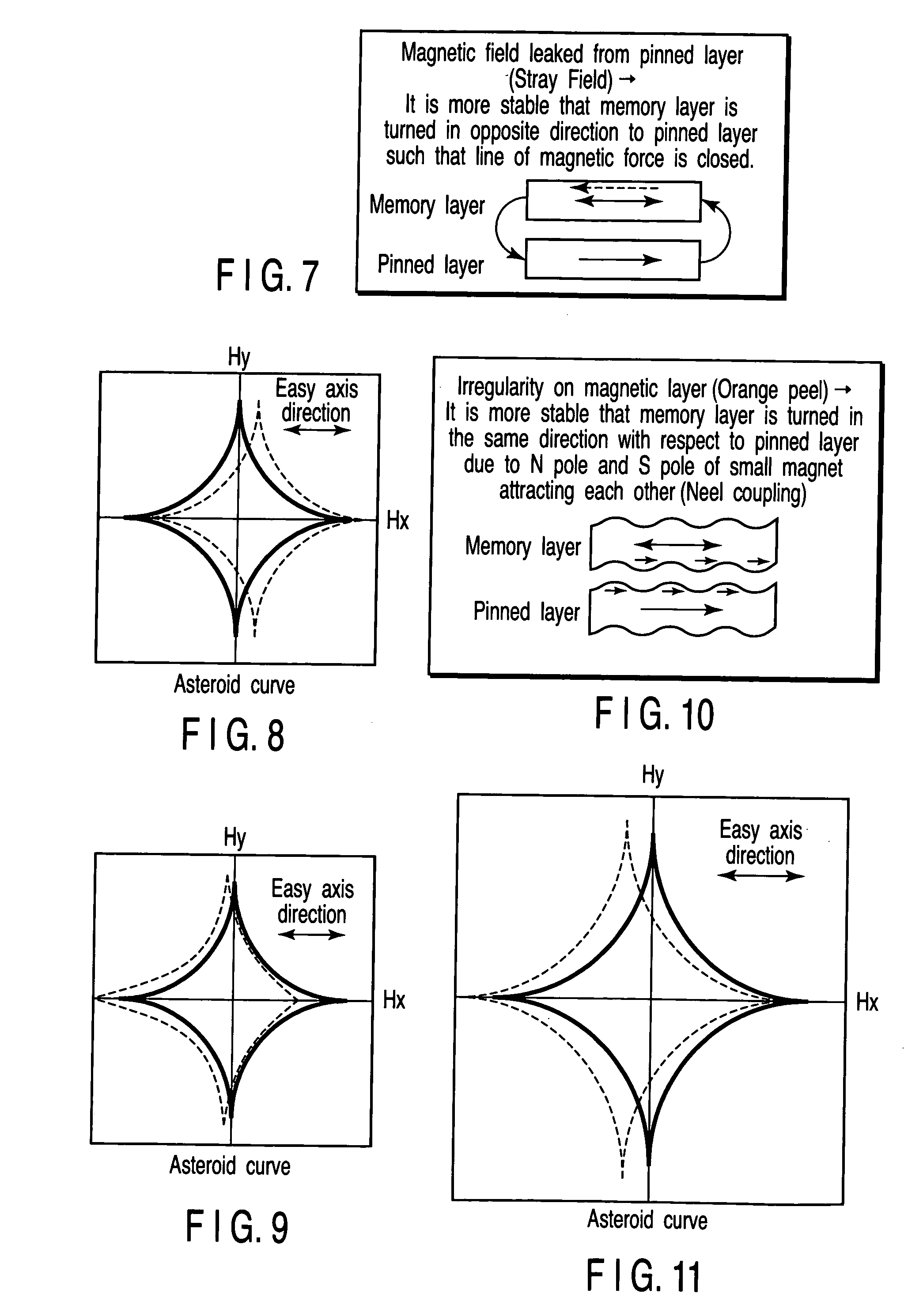
[0147] In the first embodiment described above, a state is established in which it is difficult to bring about magnetization inversion by applying a stress to the half-selected MTJ element MTJ.
[0148] In a second embodiment of the invention, with a state in which a stress is being applied to the MTJ element MTJ being as an initial state, the magnetization inversion on the half-selected MTJ element is selectively made great by eliminating the stress from the half-selected MTJ element MTJ.
A. Memory Cell
[0149] A structure of a memory cell of a magnetic random access memory according to the second embodiment is as shown in FIG. 12, and because this is the same as in the above-described first embodiment, here, description thereof will be omitted.
B. Memory Cell Array
[0150] Because the memory cell array of the magnetic random access memory according to the second embodiment is, as shown in FIG. 12, the same as in the above-described first embodiment, here, descri...
third embodiment
(3) Third Embodiment
[0165] A third embodiment of the invention relates to the toggle writing (Savtchenko) method disclosed in, for example, U.S. Pat. No. 6,545,960 and [M. Durlam, et. al., “A 0.18 μm 4 Mb Toggling MRAM” IEDM2003 Technical Digest, pp. 995-997, December 2003].
[0166] The toggle writing method has been known as a writing method in which the writing selectivity is high and it is difficult to bring about error writing. However, there is the problem that a switching magnetic field, i.e., a switching magnetic field needed for inverting a magnetized state of a selected MTJ element which will be a writing object is great.
[0167] Then, due to the example of the present invention being applied to the toggle writing method, the switching magnetic field is made little while maintaining the writing selectivity, and an attempt is made to lower an electric current consumption by reducing a write current.
A. Memory Cell
[0168] A structure of a memory cell of a magnetic random acces...
PUM
 Abstract
Description
Claims
Application Information
 - R&D
- Intellectual Property
- Life Sciences
- Materials
- Tech Scout
- Unparalleled Data Quality
- Higher Quality Content
- 60% Fewer Hallucinations
Browse by: Latest US Patents, China's latest patents, Technical Efficacy Thesaurus, Application Domain, Technology Topic, Popular Technical Reports.
© 2025 PatSnap. All rights reserved.Legal|Privacy policy|Modern Slavery Act Transparency Statement|Sitemap|About US| Contact US: help@patsnap.com