Display device and driving method thereof

a technology of a display device and a driving method, which is applied in the direction of static indicating devices, electroluminescent light sources, instruments, etc., can solve the problems of difficult to ensure the sufficient mobility of electrons, drawbacks attributed to vth shifts, etc., and achieve the effect of suppressing brightness irregularities over a whole screen

Active Publication Date: 2006-06-15
SAMSUNG DISPLAY CO LTD
View PDF6 Cites 55 Cited by
  • Summary
  • Abstract
  • Description
  • Claims
  • Application Information

AI Technical Summary

Benefits of technology

[0016] Particularly, it is found out that when amorphous silicon, for example, is used for forming a semiconductor layer of the drive switching element, the mobility of electrons in amorphous silicon is lower than the mobility of electrons in poly-silicon and hence, it is necessary to take any countermeasure to enhance the mobility of electrons in amorphous silicon.
[0017] The present invention has been made under such circumstances and it is an object of the present invention to provide a display device which allows respective pixels to emit desired quantities of light from respective pixels by suppressing a Vth shift of drive switching elements.
[0018] Further, it is another object of the present invention to provide a display device which ensures a sufficient current quantity for obtaining given light emitting quantities by driving organic EL elements through drive switching elements thus suppressing the brightness irregularities over a whole screen.

Problems solved by technology

Particularly, it is found that when an N-channel-type switching element is used as the drive switching element, a drawback attributed to the Vth shift becomes apparent.
Further, the drive switching element is formed on a portion of a pixel region and hence, a region for forming the drive switching elements is limited to ensure a sufficient light quantity whereby it is difficult to ensure the sufficient mobility of electrons.

Method used


Image

  • Display device and driving method thereof
  • Display device and driving method thereof
  • Display device and driving method thereof

Examples


embodiment 1

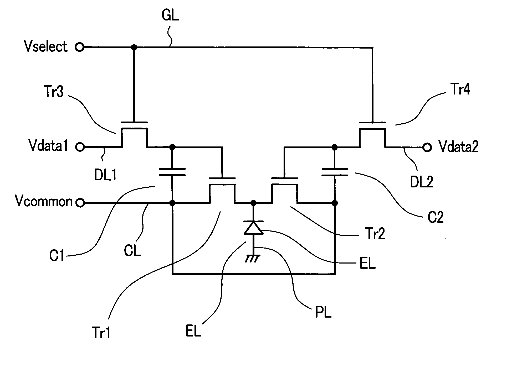
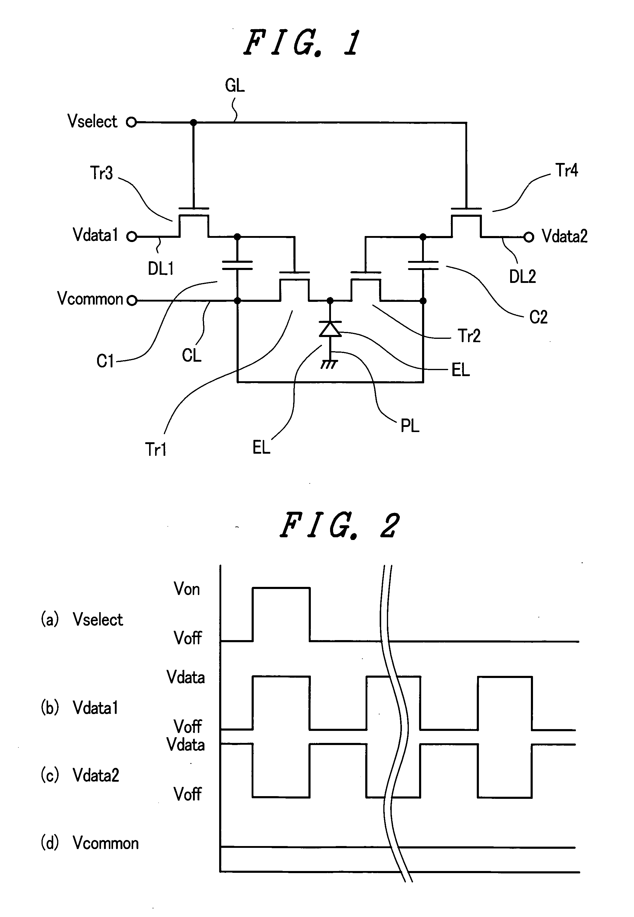
[0052]FIG. 1 is an equivalent circuit diagram showing one embodiment of the constitution of a pixel of a display device according to the present invention. As an embodiment of the display device, for example, an active-matrix-type organic EL display device is described.

[0053] Accordingly, respective pixels are arranged in a matrix array, wherein a pixel group of respective pixels arranged in parallel in the x direction adopt a gate signal line GL described later in common, and a pixel group of respective pixels arranged in parallel in the y direction adopt a first data signal line DL1 and a second data signal line DL2 in common.

[0054] Here, a first switching element Tr1 to a fourth switching element Tr4 which are used in the equivalent circuit are constituted of an N-channel-type MIS (Metal Insulator Semiconductor) transistor, for example.

[0055] In FIG. 1, first of all, the N-channel-type MIS transistor includes, first of all, the third switching element Tr3 and the third switchi...

embodiment 2

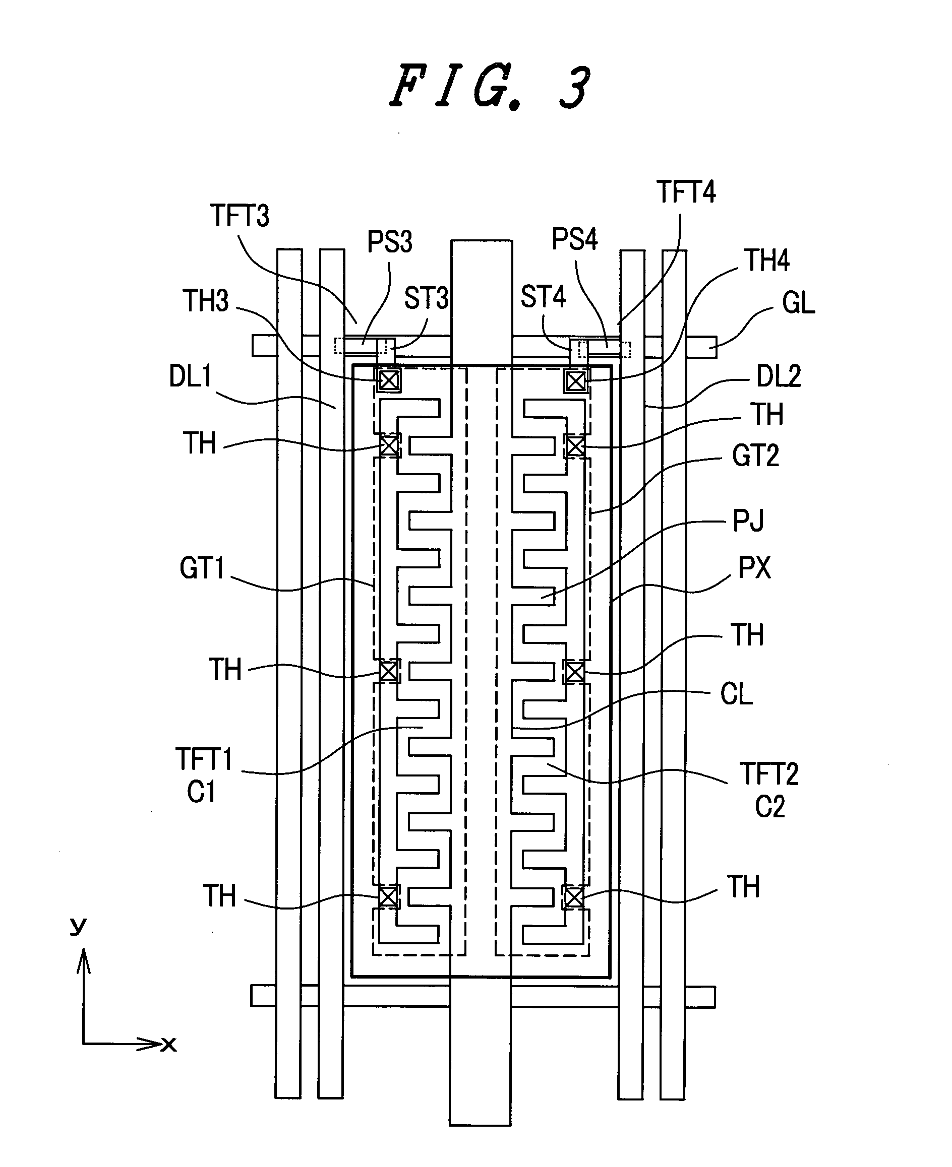
[0109]FIG. 4 is an equivalent circuit diagram showing another embodiment of the constitution of the pixel of the display device according to the present invention and corresponds to FIG. 1.

[0110] The constitution which makes this embodiment different from the embodiment shown in FIG. 1 lies in that, first of all, each pixel uses one data signal line DL and uses two gate signal lines GL instead of one gate signal line GL.

[0111] In a color display, for example, three pixels which are arranged close to each other in the running direction of the gate signal line GL are configured to emit lights of respective colors consisting of red (R), green (G), blue (B), and these respective pixels constitute a unit pixel of the color display.

[0112] In the equivalent circuit shown in FIG. 1, six data signal lines DL in total become necessary. However, by increasing one gate signal line GL which is formed in common with the respective pixels, it is possible to obtain an advantageous effect that th...


PUM


Abstract

The present invention enhances a display quality of a display device as a task. As means for solving such a task, the present invention provides a display device including a light emitting element and a switching element in a pixel, wherein the switching element is provided for supplying a power source to the light emitting element and is constituted of a first switching element and a second switching element. The first switching element and the second switching element are configured to be operated, in response to inputting of data signals into the inside of the pixel, one switching element assumes a positive bias state and another switching element assumes a reverse bias state, and the bias states are alternately changed over between the first switching element and the second switching element in response to time-sequential inputting of the data signals, and the supply of the power source to the light emitting element is performed by way of either one of the first switching element and the second switching element.

Description

CROSS-REFERENCE TO RELATED APPLICATIONS [0001] The disclosure of Japanese Patent Application No. JP2004-355401 filed on Dec. 08, 2004 including the specification, drawings and abstract is incorporated herein by reference in its entirety. BACKGROUND OF THE INVENTION [0002] 1. Field of the Invention [0003] The present invention relates to a display device and a driving method thereof, for example, an organic EL display device and a driving method thereof. [0004] 2. Description of the Related Art [0005] An active-matrix-type organic EL display device is, for example, configured such that respective pixels which are arranged in parallel in the x direction are selected in response to scanning signals and data signals are supplied to respective pixels in conformity with the selection timing. [0006] In each pixel to which the data signal is supplied, the data signal is stored in a capacitive element, a switching element (a drive switching element) is driven by the stored charge, and a powe...

Claims


Application Information

Patent Timeline
Patent Type & Authority Applications(United States)
IPC IPC(8): G09G3/30
CPCG09G3/3233G09G2300/0823G09G2320/0233G09G2320/043G09G3/30H05B33/12
Inventor TANAKA, MASAHIROMATSUURA, TOSHIYUKIMURAKAMI, HAJIMEAKIMOTO, HAJIME
Owner SAMSUNG DISPLAY CO LTD
Why Eureka
Try Eureka