Memory device, memory controller and method for operating the same

a memory controller and memory array technology, applied in the memory field, can solve the problems of inability to operate the computer system using the memory device, the minimum time between data read accesses to different columns of the memory array is limited, and the amount of data read out is too larg

Inactive Publication Date: 2006-06-15
INFINEON TECH AG
View PDF26 Cites 85 Cited by
  • Summary
  • Abstract
  • Description
  • Claims
  • Application Information

AI Technical Summary

Benefits of technology

[0009] Such a memory device may include separated arrangements of sets of memory banks, each having its own internal data buses and internal command and address buses. All of the command and address buses are connected to the command and address unit which directs the received command and address data to the respective set of memory banks. Similarly, the data buses are separately connected to the data output unit in which the data read out during the data access are buffered and serially output. Buffering and outputing data serially may be performed as commonly known for data accesses. The physically separated arrangements of the sets of memory banks (each connected to its own data and command bus and address bus) allow the data banks to be operated separately substantially without considering any minimum access time, such as the column-to-column delay (tCCD), which defines the time between successive column accesses.
[0023] The step of sorting of the requests with respect to their addresses may be performed so that the short time interval is set to a time determined by the column access cycle time divided by the number of sets of memory banks in the memory device. This allows for rapidly sending read requests to the memory device wherein each read request may initiate a burst read-out in one set of memory banks within the memory device and wherein the data provided by each set of memory banks is serially output.

Problems solved by technology

Thereby, depending on the configuration of the memory device, it is possible that the amount of data read out within a data access is too large and cannot be used by the computer system the memory device is operated in.
However, the minimum time between the data read accesses to different columns of the memory array is limited by the currently used dynamic random access memory (DRAM) technology and by the DRAM array architecture.
This means that successive read requests to different columns of the memory device cannot be supplied to the memory array in shorter time than determined by the so called column access cycle time.
In conventional memory devices, therefore, read requests to different columns of the memory array cannot be applied faster than the column access cycle time wherein an amount of data is serially output during the whole column access cycle time.
However, reducing the amount of data output within the column access cycle time would result in a time gap between the last data bit to be output and the time at which the next data access delivers data to be output from the memory device.

Method used


Image

  • Memory device, memory controller and method for operating the same
  • Memory device, memory controller and method for operating the same
  • Memory device, memory controller and method for operating the same

Examples


Embodiment Construction

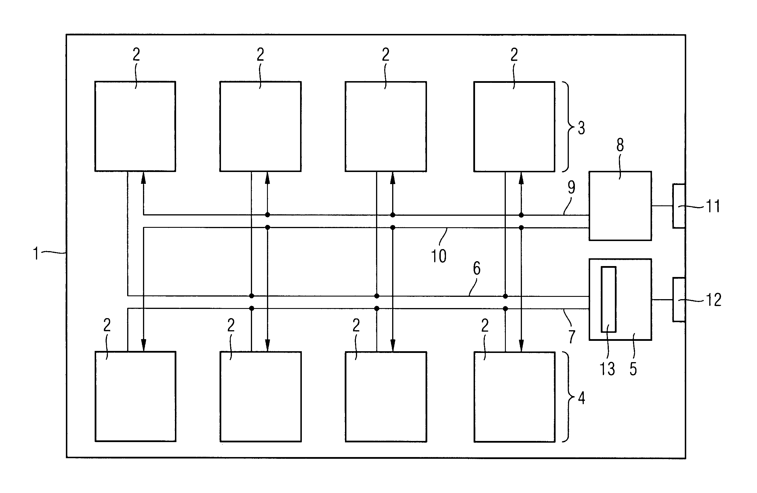
[0027] In FIG. 1, a block diagram of a memory device 1 according to one embodiment of the present invention is depicted. The memory device 1 includes a plurality of memory banks 2 which are grouped into different sets of memory banks (also referred herein as “memory banks set”). In the given example, a first set 3 of memory banks 2 and a second set 4 of memory banks 2 are depicted, each set of memory banks including four memory banks 2. The memory banks 2 include one or more memory arrays and may be equal in size. However, different sizes of memory arrays may be utilized. The memory arrays may include DRAM memory cells, thereby forming a DRAM memory. Other types of memory cells are also applicable if they have access time restrictions as is usually the case in DRAM memory cells.

[0028] The memory arrays comprise a matrix of DRAM memory cells arranged on wordlines and bitlines (or row lines and column lines) by which the DRAM memory cells can be selected and addressed. In a read acce...


PUM


Abstract

One embodiment of the present invention provides a memory device comprising a plurality of sets of memory banks, wherein each memory bank includes a memory array and is adapted to be read out in a data access; a plurality of internal data buses and a plurality of internal command and address buses connected to the plurality of sets of memory banks, respectively, such that each set of memory banks is associated with one of the internal data buses and one of the internal command and address buses; a command and address port for receiving command and address data from outside; and a command and address unit to direct the received command and address data to one of the sets of memory banks via the associated command and address bus, depending on the address data; and a data output unit for receiving data read out from one set of memory banks via the respective internal data bus in the data access and for serially outputting the received data.

Description

BACKGROUND OF THE INVENTION [0001] 1. Field of the Invention [0002] The present invention relates to a memory device including memory banks having one or more memory arrays from which data can be read out. The present invention also relates to a memory controller adapted to control a connected memory device. The present invention further relates to methods for controlling such a memory device and such a memory controller. [0003] 2. Description of the Related Art [0004] Memory devices usually provide that data stored therein can be read out in a data access, e.g., a number of data is simultaneously read out at a determined row and column of the memory device and output at least partially in series within a burst time interval before the next read address can be applied to the memory device to read out further data in a next data access. With conventional Double-Data-Rate (DDR) technology, the data rate by which data is read out from the memory device is increased as data is output wi...

Claims


Application Information

Patent Timeline
Patent Type & Authority Applications(United States)
IPC IPC(8): G06F12/06
CPCG06F13/1631G11C7/1012G11C7/1051G11C7/1069G11C8/12G11C11/4093G11C2207/107
Inventor RUCKERBAUER, HERMANNSICHERT, CHRISTIANSAVIGNAC, DOMINIQUE
Owner INFINEON TECH AG
Why Eureka
Try Eureka