Nonvolatile memory device having two or more resistance elements and methods of forming and using the same

a technology of resistance elements and memory devices, which is applied in the direction of digital storage, semiconductor devices, instruments, etc., can solve the problems of affecting the processing efficiency of the device, the loss of stored data of the device, and the detriment of the integration density and/or the operation speed

Active Publication Date: 2006-06-22
SAMSUNG ELECTRONICS CO LTD
View PDF4 Cites 105 Cited by
  • Summary
  • Abstract
  • Description
  • Claims
  • Application Information

AI Technical Summary

Problems solved by technology

However, a DRAM's stored data is lost when power is cut off.
A flash memory device is nonvolatile, unlike a volatile memory device, but may have detriments of a lower integration density and / or a lower operation speed, as compared to a DRAM.
When a conventional fabrication process of a DRAM is employed to fabricate a PRAM, etching is difficult and it may take a long time.
Further, conventional memory devices may have a problem of achieving a precise switching operation because its structure is complicated when switching using a transistor or diode.

Method used


Image

  • Nonvolatile memory device having two or more resistance elements and methods of forming and using the same
  • Nonvolatile memory device having two or more resistance elements and methods of forming and using the same
  • Nonvolatile memory device having two or more resistance elements and methods of forming and using the same

Examples


example electrical

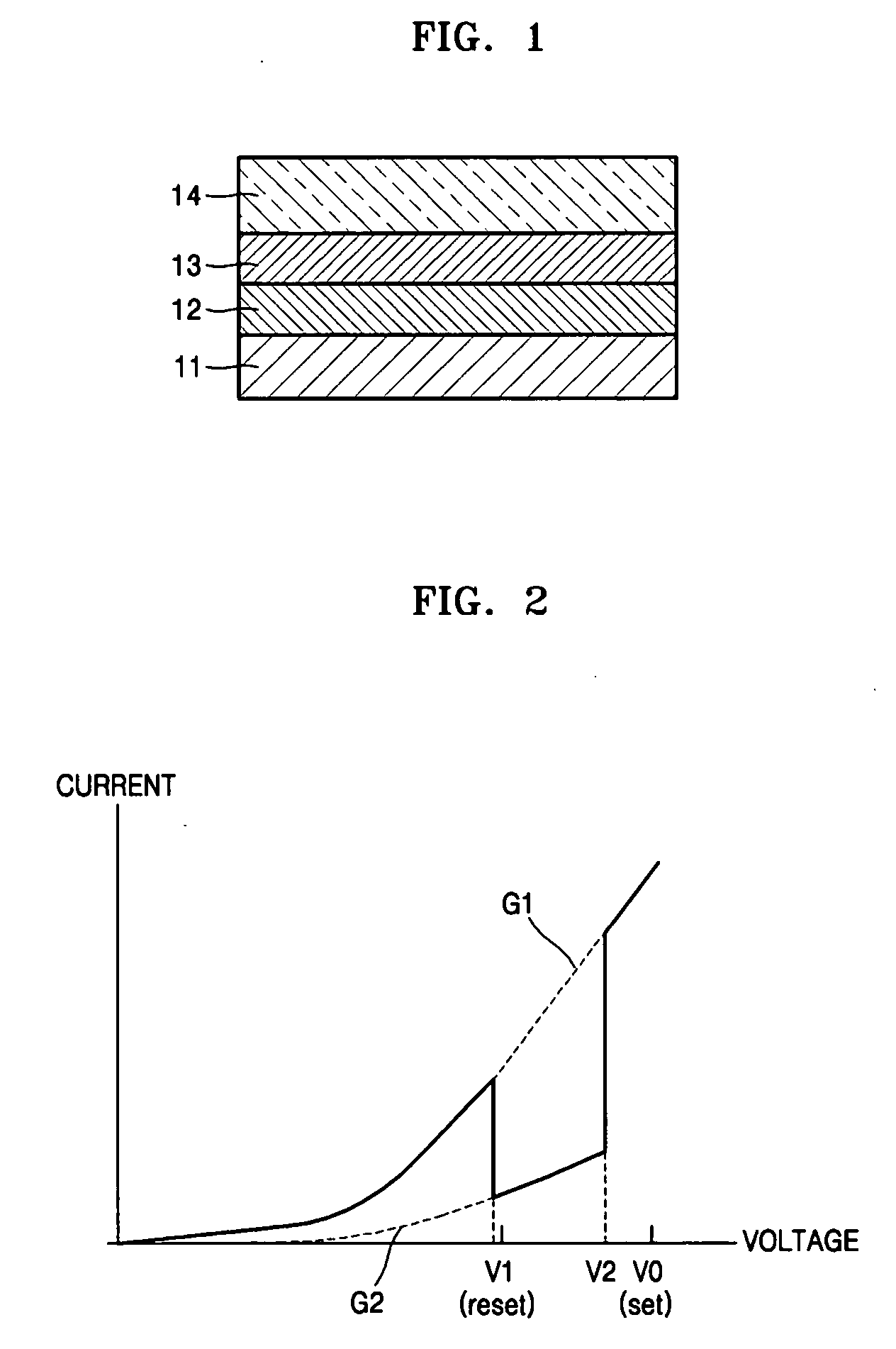
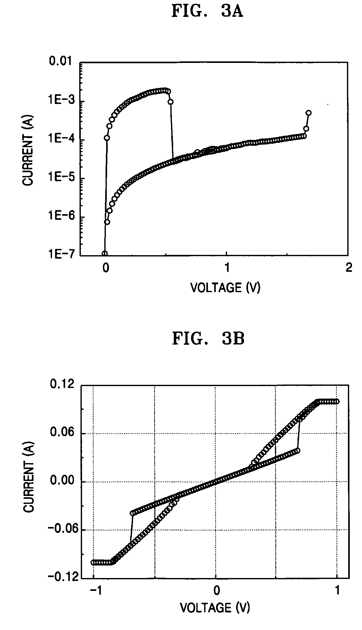
[0054] Example electrical characteristic graphs of the materials used in the first resistance layer 12 and the second resistance layer 13 are shown in FIGS. 3A through 3C.

[0055]FIG. 3A is a graph illustrating electrical characteristics of Ni1-xOx used for the first resistance layer 12. FIG. 3A illustrates two resistance characteristics in a voltage range equal to or lower than about 0.55 V. That is, because Ni1-xOx shows two resistance characteristics at a same applied voltage, it can be used as a data storage part of a memory device.

[0056]FIG. 3B is a graph illustrating electrical characteristics of V2O5 used for the second resistance layer 13 according to an example embodiment of the present invention and FIG. 3C is a graph illustrating electrical characteristics of TiAlO3 used for the second resistance layer 13 according to an example embodiment of the present invention. Referring to FIGS. 3B and 3C, these have various voltage-current states, and particularly, current flows by a...


PUM


Abstract

A nonvolatile memory device having two or more resistors and methods of forming and using the same. A nonvolatile memory device having two resistance layers, and more particularly, to a nonvolatile memory device formed and operated using a resistance layer having memory switching characteristics and a resistance layer having threshold switching characteristics. The nonvolatile semiconductor memory device may include a lower electrode; a first resistance layer having at least two resistance characteristics formed on the lower electrode, a second resistance layer having threshold switching characteristics formed on the first resistance layer, and an upper electrode formed on the second resistance layer.

Description

PRIORITY STATEMENT [0001] This application claims the benefit of Korean Patent Application No. 10-2004-0109268, filed on Dec. 21, 2004, in the Korean Intellectual Property Office, the disclosure of which is incorporated herein in its entirety by reference. BACKGROUND [0002] 1. Field [0003] Example embodiments of the present invention relate to a nonvolatile memory device having two resistance elements, and more particularly, to a nonvolatile memory device formed and operated using a resistance element having memory switching characteristics and a resistance element having threshold switching characteristics. [0004] 2. Description of the Related Art [0005] A good semiconductor memory device must have a high integration density, which means that the number of memory cells per unit area is high, a high operation speed and / or a drive capability at low power. Thus, many efforts have been made to develop such a semiconductor device, and various kinds of memory devices are produced. [0006]...

Claims


Application Information

Patent Timeline
Patent Type & Authority Applications(United States)
IPC IPC(8): H01L29/02
CPCG11C13/0004G11C13/0007G11C13/003G11C2213/31G11C2213/32G11C2213/56G11C2213/76G11C2213/77H01L27/2427H01L45/04H01L45/1233H01L45/146H01L27/2463H10B63/24H10B63/80H10N70/20H10N70/826H10N70/8833
Inventor JOUNG, YOUNG-SOOPARK, YOON-DONGYOO, IN-KYEONGLEE, MYOUNG-JAESEO, SUN-AEKIM, HYE-YOUNGAHN, SEUNG-EONSEO, DAVID
Owner SAMSUNG ELECTRONICS CO LTD
Why Eureka
Try Eureka