Semiconductor device having overlay measurement mark and method of fabricating the same

a technology of semiconductor devices and measurement marks, which is applied in the direction of semiconductor/solid-state device testing/measurement, instruments, photomechanical equipment, etc., can solve the problems of reducing the size of overlay measurement marks, increasing the possibility of producing defective semiconductor devices, and limiting the development of overlay measurement marks. , to achieve the effect of preventing an overlay failure and reducing the error rang

Active Publication Date: 2006-06-22
SAMSUNG ELECTRONICS CO LTD
View PDF10 Cites 12 Cited by
  • Summary
  • Abstract
  • Description
  • Claims
  • Application Information

AI Technical Summary

Benefits of technology

[0016] Therefore, the present invention provides a semiconductor device and a method of fabricating the same having an overlay measurement mark being suitable to preventing an overlay failure in a photolithogra...

Problems solved by technology

As described above, in the case that the shape of the main scale is distorted due to procedure problems since one measurement mark exists in one region in the conventional box-type or frame-type, a possibility of producing defective semiconductor devices is increased because the measurement of an overlay is not made prec...

Method used


Image

  • Semiconductor device having overlay measurement mark and method of fabricating the same
  • Semiconductor device having overlay measurement mark and method of fabricating the same
  • Semiconductor device having overlay measurement mark and method of fabricating the same

Examples


Embodiment Construction

[0041] The present invention will now be described more fully hereinafter with reference to the accompanying drawings, in which preferred embodiments of the invention are shown. In the drawings, the thicknesses of layers and regions are exaggerated for clarity.

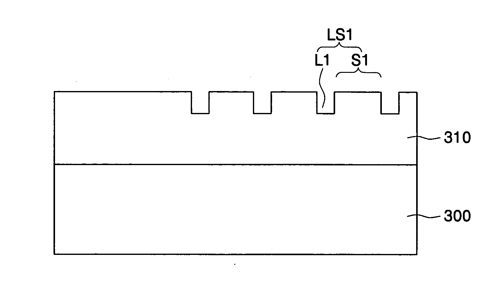
[0042]FIGS. 3A and 4A are plan views illustrating a method of fabricating a semiconductor device having an overlay measurement mark according to an embodiment of the present invention. FIGS. 3B and 4B are sectional views taken along a line of II-II′ of FIGS. 3A and 4A, respectively.

[0043] Referring to FIGS. 3A and 3B, a scribe line region is defined on a semiconductor substrate 300. A lower layer is formed on the semiconductor substrate 300 of the scribe line region. The lower layer is patterned, thereby forming a main scale layer 310 having vertical line and space patterns LS1 and horizontal line and space patterns LS2. The vertical line and space patterns LS1 and the horizontal line and space patterns LS2 may be formed nea...


PUM


Abstract

There are provided a semiconductor device having an overlay measurement mark, and a method of fabricating the same. The semiconductor device includes a scribe line region disposed on a semiconductor substrate. A first main scale layer having a first group of line and space patterns and a second group of line and space patterns is disposed on the scribe line region. Line-shaped second main scale patterns are disposed on space regions of the first group of the line and space patterns. Line-shaped vernier scale patterns are disposed on space regions of the second group of the line and space patterns. In the method, a first main scale layer having a first group of line and space patterns and a second group of line and space patterns is formed on a semiconductor substrate. Line-shaped second main scale patterns are formed on space regions of the first group of the line and space patterns. Line-shaped vernier scale patterns are formed on space regions of the second group of the line and space patterns.

Description

CROSS-REFERENCE TO RELATED APPLICATION [0001] This application claims priority from Korean Patent Application No. 2004-109903, filed on Dec. 21, 2004, the contents of which are hereby incorporated herein by reference in their entirety as if set forth fully herein. BACKGROUND OF INVENTION [0002] 1. Technical Field [0003] The present invention relates to a semiconductor device and a method of fabricating the same, and more particularly, to a semiconductor device having an overlay measurement mark and a method of fabricating the same. [0004] 2. Discussion of the Related Art [0005] With semiconductor devices being highly integrated in recent years, a density of patterns formed on a wafer is increased. Specifically, a pattern density in a cell region is very high in comparison with that of a peripheral circuit region. The device elements formed in the cell region or the peripheral circuit region are formed by repeatedly performing processes, such as thin film deposition, a photolithograp...

Claims


Application Information

Patent Timeline
IPC IPC(8): H01L23/58
CPCG03F7/70633G03F9/7076H01L23/544H01L2223/54453H01L2924/0002H01L2924/00G03F9/7084H01L22/30
Inventor KOH, CHA-WONWOO, SANG-GYUNOH, SEOK-HWANYEO, GI-SUNGKANG, HYUN-JAESHIN, JANG-HO
Owner SAMSUNG ELECTRONICS CO LTD
Why Eureka
Try Eureka