Semiconductor integrated circuit device formed by automatic layout wiring by use of standard cells and design method of fixing its well potential

a technology of automatic layout and integrated circuit device, which is applied in the direction of computer aided design, cad circuit design, basic electric elements, etc., can solve the problems of reducing the driving capability, reducing the minimum distance or the like of the mos transistor formed in the well region, and reducing the step coating property

Inactive Publication Date: 2006-06-22
KK TOSHIBA
View PDF1 Cites 152 Cited by
  • Summary
  • Abstract
  • Description
  • Claims
  • Application Information

AI Technical Summary

Benefits of technology

[0018]FIG. 4 is a flowchart to help explain a design method of forming the semiconductor integrated circuit device of FIG. 1;
[0019]FIG. 5 is a flowchart to help explain a method of designing a semiconductor integrated circuit device according to a second embodiment of the present invention;
[0020]FIG. 6 is a block diagram of an image drawing processor system LSI to help explain an application of a semiconductor integrated circuit device and its design method according to the first and second embodiments; and
[0021]FIG. 7 is a block diagram to help explain a detailed configuration of the graphic processor in the circuit of FIG. 6.

Problems solved by technology

To prevent the cell area from increasing, the sizes of semiconductor elements, including transistors, formed in the cell have to be reduced, resulting in a decrease in the driving capability.
Particularly when the sub-regions and their interconnections are formed with the minimum line width according to design rules, the minimum distance or the like for the MOS transistors formed in the well region is limited or the step coating property is degraded.
In addition, contact with the densely arranged sub-regions necessitates complicated manufacturing processes.
If there are a lot of such patterns, this results in a drop in the manufacturing yield.

Method used


Image

  • Semiconductor integrated circuit device formed by automatic layout wiring by use of standard cells and design method of fixing its well potential
  • Semiconductor integrated circuit device formed by automatic layout wiring by use of standard cells and design method of fixing its well potential
  • Semiconductor integrated circuit device formed by automatic layout wiring by use of standard cells and design method of fixing its well potential

Examples


first embodiment

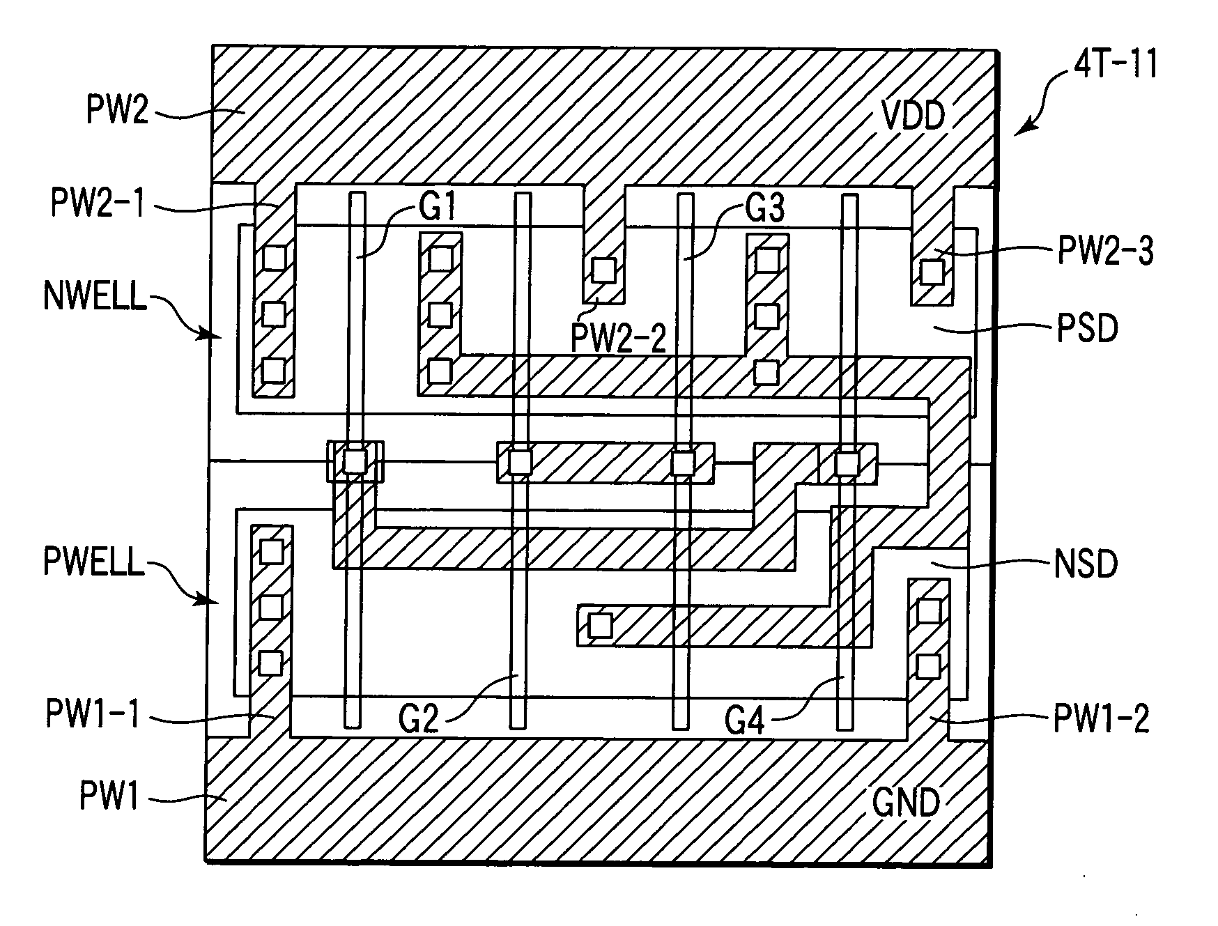
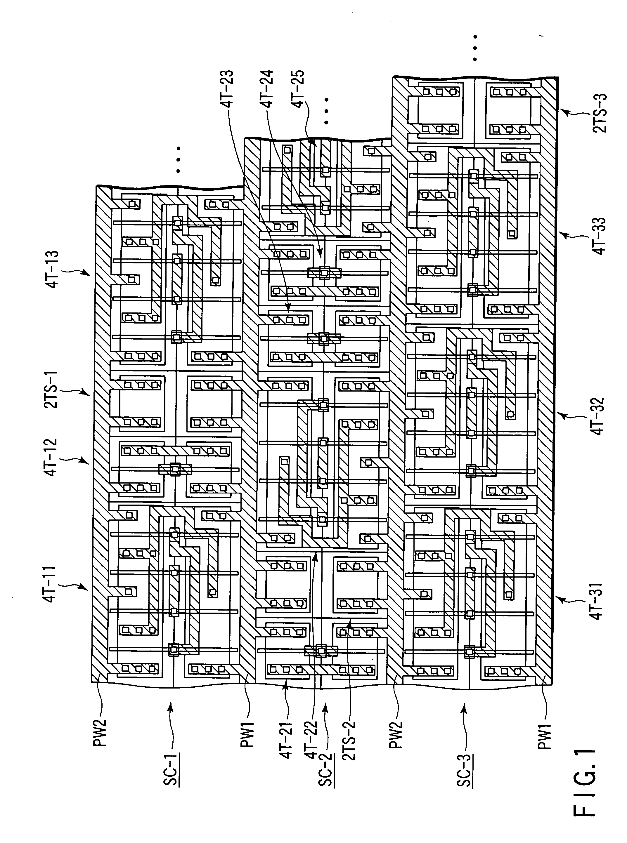
[0022]FIG. 1 is a plan view showing a pattern configuration to help explain a semiconductor integrated circuit device according to a first embodiment of the present invention. FIG. 1 shows a layout image example by extracting a part of the circuit pattern in a semiconductor integrated circuit device formed by automatic layout wiring by use of standard cells.

[0023] In a layout example of FIG. 1, three stages of cell columns SC-1, SC-2, SC-3 are arranged. The adjacent cell columns SC-1, SC-2 share an interconnection (power supply line) PW1. The adjacent cell columns SC-2, SC-3 share an interconnection (power supply line) PW2. The power supply line PW2 is for, for example, the power supply voltage VDD. The power supply line PW1 is for, for example, the ground potential GND. Each of the power supply lines PW1, PW2 includes a branch section extending into the cell so as to face the corresponding branch section of the other. These branch sections are connected via contact holes to the se...

second embodiment

[0046]FIG. 5 is a flowchart to help explain a method of designing a semiconductor integrated circuit device according to a second embodiment of the present invention. The second embodiment optimizes the operation timing of the circuit by replacing a part of the circuit composed of 4-terminal cells with 2-terminal cells and produces the same effect as the first embodiment.

[0047] First, a 4-terminal standard cell is read from a library and a temporary circuit is composed of (temporarily configured using) only 4-terminal standard cells by automatic layout wiring (STEP 1).

[0048] Next, the operation timing of the temporary circuit formed is measured (STEP 2).

[0049] Thereafter, the measured operation timing is judged (STEP 3).

[0050] Next, a timing adjustment optimum value is calculated on the basis of the judged operation timing (STEP 4).

[0051] Then, on the basis of the calculated timing adjustment optimum value, a 2-terminal standard cell is read from the library. Timing adjustment ...


PUM


Abstract

A standard cell is read from a library and automatic layout wiring is performed, thereby configuring a circuit. Next, each cell column in the configured circuit is searched for an empty region. In the empty region in the cell column searched for, a spacer cell or a filler cell is placed. At this time, using the spacer cell or filler cell, the well potential of the standard cells in the cell column is fixed.

Description

CROSS-REFERENCE TO RELATED APPLICATIONS [0001] This application is based upon and claims the benefit of priority from prior Japanese Patent Application No. 2004-366438, filed Dec. 17, 2004, the entire contents of which are incorporated herein by reference. BACKGROUND OF THE INVENTION [0002] 1. Field of the Invention [0003] This invention relates to a semiconductor integrated circuit device and its design method, and more particularly to the technique for fixing the well potential in a semiconductor integrated circuit device formed by automatic layout wiring by use of standard cells. [0004] 2. Description of the Related Art [0005] It is known that the element characteristics of the transistors formed in a semiconductor integrated circuit device, such as an IC or an LSI, are influenced by fluctuations in the well potential. To avoid such influence and stabilize the element characteristics of the transistors, it is necessary to stabilize (fix) the well potential. [0006] In a semiconduc...

Claims


Application Information

Patent Timeline
Patent Type & Authority Applications(United States)
IPC IPC(8): H01L27/10
CPCG06F17/5068H01L27/0207H01L27/11807Y10S257/909G06F30/39
Inventor KINOSHITA, KOICHIITAKA, YASUHITOSUGAHARA, TAKESHI
Owner KK TOSHIBA
Why Eureka
Try Eureka