
System and process for processing a plurality of semiconductor thin films which are crystallized using sequential lateral solidification techniques

a semiconductor and sequential solidification technology, applied in the field of semiconductor thin film system and process, can solve the problems of affecting the uniformity of the thin film sample, affecting the uniformity of the thin film transistor (“tft”) device, and requiring approximately 200 second to 600 second to complete the semiconductor film sample processing, so as to prevent or delay the irradiation of the second sample

Inactive Publication Date: 2006-06-22
THE TRUSTEES OF COLUMBIA UNIV IN THE CITY OF NEW YORK
View PDF98 Cites 25 Cited by
  • Summary
  • Abstract
  • Description
  • Claims
  • Application Information

AI Technical Summary

Benefits of technology

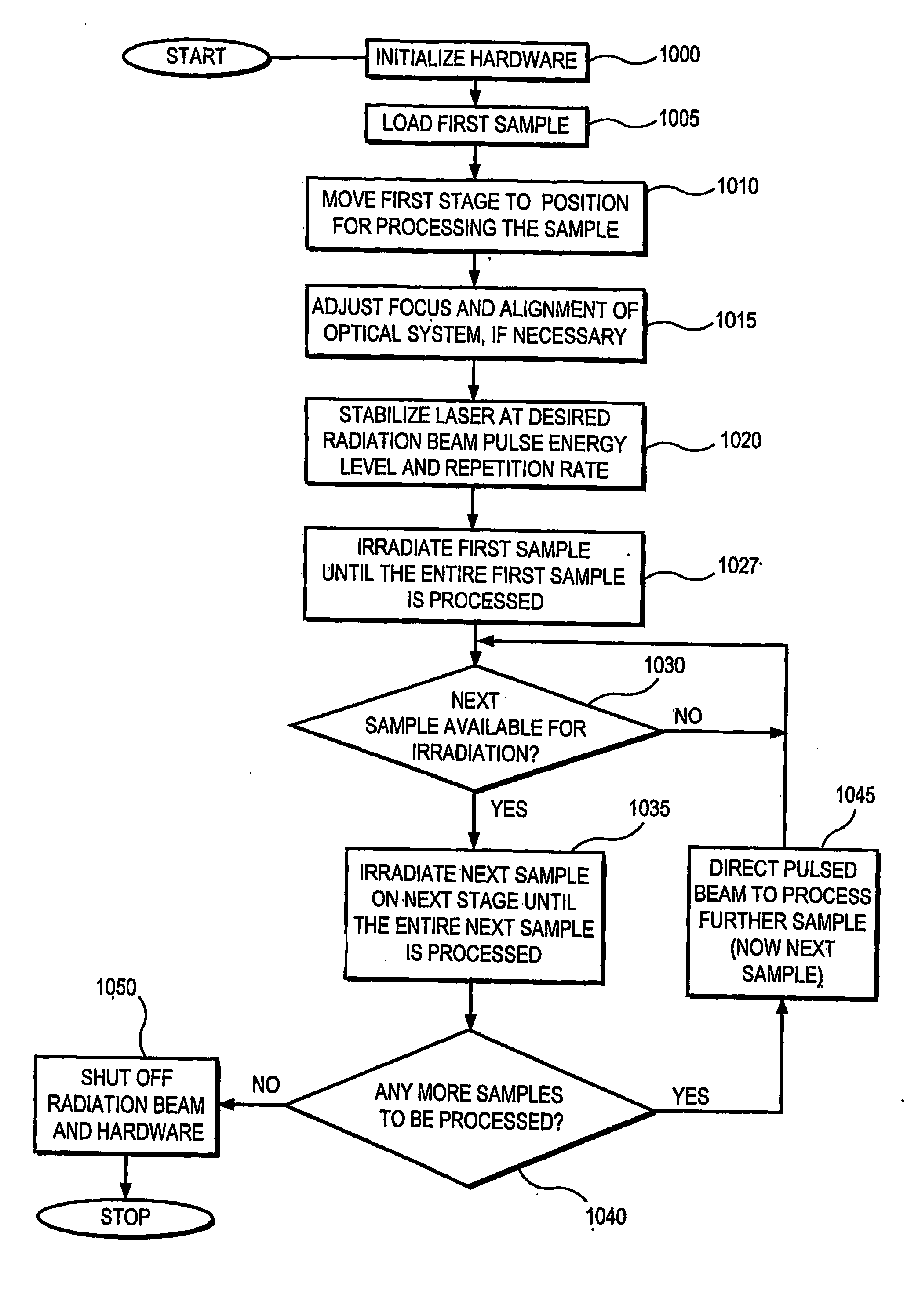
The present invention provides systems and processes for sequentially processing semiconductor film samples by irradiating and melting them, and allowing them to solidify and crystallize. The systems and processes allow for the unloading of a previously-processed sample and the loading of an unprocessed sample without shutting down the pulsed beam. The invention also allows for the use of different techniques for processing the samples, and the redirection of beam pulses for the second sample based on the outcome of the first sample. The technical effects of the invention include improved efficiency and accuracy in the processing of semiconductor film samples.

Problems solved by technology

However, the semiconductor films processed using such known ELA methods often suffer from microstructural non-uniformities such as edge effects, which manifest themselves in availing a non-uniform performance of thin-film transistor (“TFT”) devices fabricated on such films.
In addition, it may take approximately 200 second to 600 seconds to completely process the semiconductor film sample using the ELA techniques, without even taking into consideration the time it takes to load and unload such sample.
Such stability may be reduced or compromised when the pulsed beams are turned off or shut down, and then restarted.
In addition, the costs associated with processing semiconductor samples are generally correlated with the number of pulses emitted by the beam source.

Method used


Image

  • System and process for processing a plurality of semiconductor thin films which are crystallized using sequential lateral solidification techniques
  • System and process for processing a plurality of semiconductor thin films which are crystallized using sequential lateral solidification techniques
  • System and process for processing a plurality of semiconductor thin films which are crystallized using sequential lateral solidification techniques

Examples


Embodiment Construction

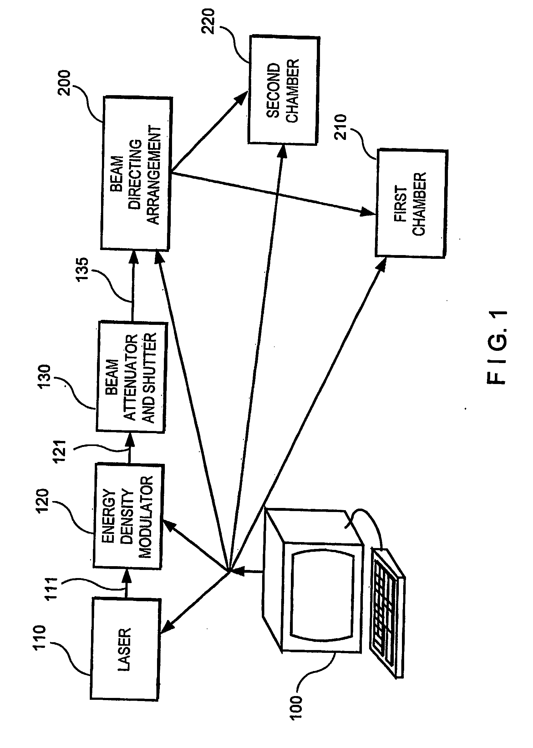
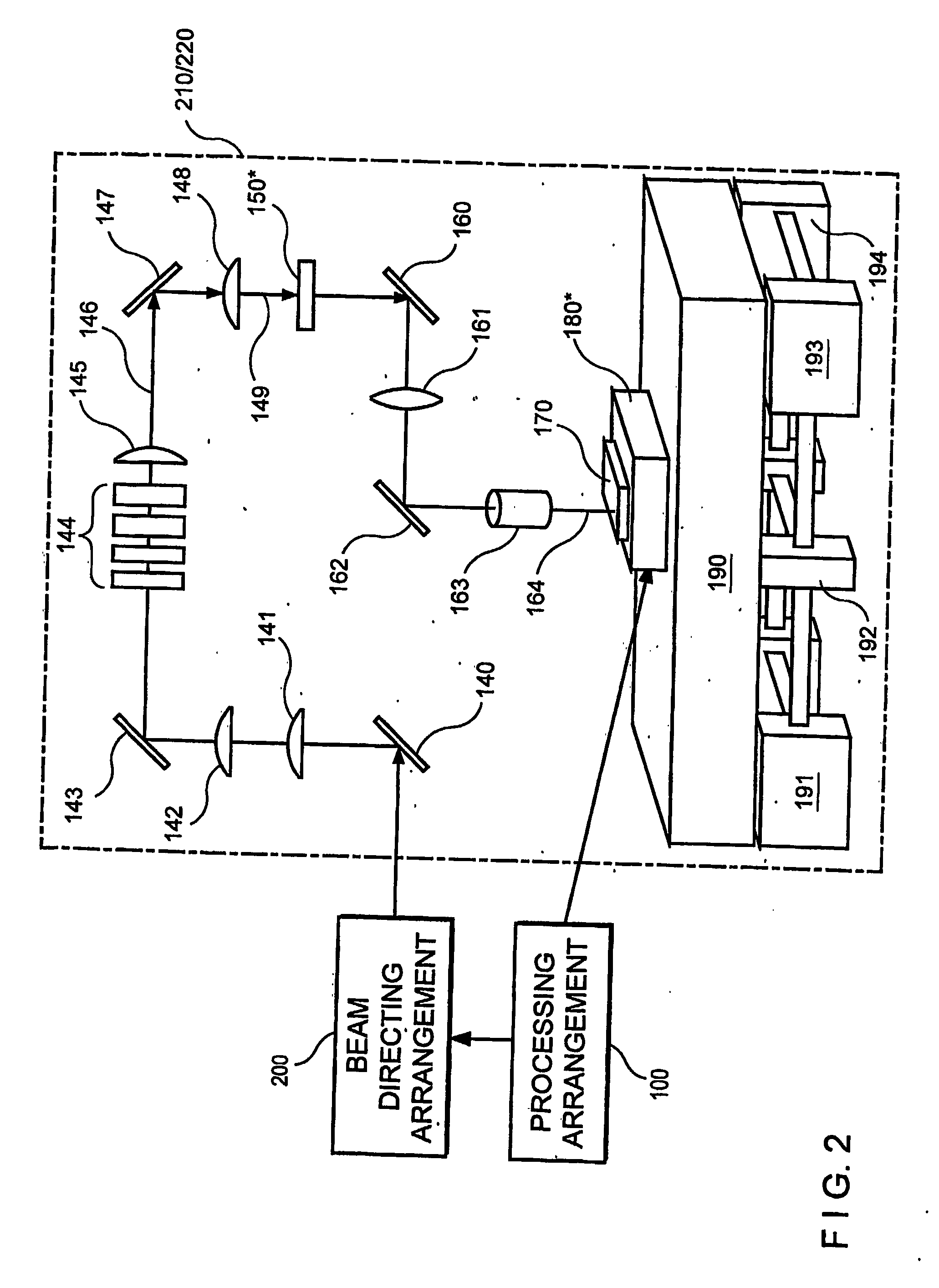
[0019] Certain systems and processes for providing continuous motion SLS are described in U.S. Pat. Nos. 6,322,625 and 6,368,945 and U.S. patent application Ser. Nos. 09 / 390,535 and 09 / 390,537. In addition, systems and processes for providing uniform small grained materials (“UGS”) techniques are described in U.S. Patent Application Serial Nos. 60 / 405,084, 60 / 405,083 and 60 / 405,085, and International Applications PCT / US03 / 25946, PCT / US03 / 25972 and PCT / US03 / 25954. Exemplary systems and processed according to the present invention can employ principles and components thereof to sequentially process a thin film of each of two or more semiconductor samples In particular, the system and process according to the present invention can be used to process two or more samples (provided on distinct stages). Each of the sample has an amorphous silicon thin film provided thereon.

[0020] In particular, as shown in FIG. 1, an exemplary embodiment of the system according to the present invention ma...


PUM

PropertyMeasurementUnit
transfer timeaaaaaaaaaa
processingaaaaaaaaaa

Abstract

A process and system are provided for processing at least one section of each of a plurality of semiconductor film samples. In these process and system, the irradiation beam source is controlled to emit successive irradiation beam pulses at a predetermined predetermined repetition rate. Using such emitted beam pulses, at least one section of one of the semiconductor film samples is irradiated using a first sequential lateral solidification (“SLS”) technique and / or a first uniform small grained material (“UGS”) techniques to process the such sections) of the first sample. Upon the completion of the processing of this section of the first sample, the beam pulses are redirected to impinge at least one section of a second sample of the semiconductor film samples. Then, using the redirected beam pulses, such sections) of the second sample are irradiated using a second SLS technique and / or a second UGS technique to process the at least one section of the second sample. The first and second techniques can be different from one another or substantially the same.

Description

FIELD OF THE INVENTION [0001] The present invention relates to a system and process for processing a plurality of semiconductor thin films (such as silicon thin films) using a pulse energy beam. In particular, one exemplary embodiment of the system and process utilizes a pulsed beam in conjunction with a sequential lateral solidification (“SLS”) technique to irradiate at least two semiconductor thin films, without stopping the emission of energy the pulsed beam. Another exemplary embodiment of the system and process also uses a pulsed beam to irradiate sections of the film such that the areas that have been irradiated and resolidified which have small-grains therein do not overlap one another, and can be used to place therein thin film transistor (“TFT”) devices. BACKGROUND INFORMATION [0002] Semiconductor films, such as silicon films, are known to be used for providing pixels for liquid crystal display devices. Such films have previously been processed (i.e., irradiated by an excim...

Claims


Application Information

Patent Timeline
Patent Type & Authority Applications(United States)
IPC IPC(8): H01L21/20H01L21/36B23K26/067B23K26/12
CPCB23K26/063B23K26/0639B23K26/0648B23K26/0665B23K26/067Y10T428/24802B23K26/12H01L21/2026B23K26/127B23K26/128Y10S117/904B23K26/0673B23K26/064B23K26/0622H01L21/02689H01L21/02686H01L21/02683H01L21/02691H01L21/02532H01L21/02678
Inventor IM, JAMES S.
Owner THE TRUSTEES OF COLUMBIA UNIV IN THE CITY OF NEW YORK
Learn More