Semiconductor package and lead frame therefor

a technology of semiconductor devices and lead frames, which is applied in the direction of semiconductor devices, semiconductor/solid-state device details, electrical apparatus, etc., can solve the problems of difficult to further improve the reliability of electric connection between qfn packages, and achieve the effect of improving reliability regarding electric connection

Inactive Publication Date: 2006-06-29
YAMAHA CORP
View PDF4 Cites 36 Cited by
  • Summary
  • Abstract
  • Description
  • Claims
  • Application Information

AI Technical Summary

Benefits of technology

[0017] When the aforementioned semiconductor package using the aforementioned lead frame is mounted onto a board h...

Problems solved by technology

In other words, under the present circumstances, it is very difficult to further imp...

Method used


Image

  • Semiconductor package and lead frame therefor
  • Semiconductor package and lead frame therefor
  • Semiconductor package and lead frame therefor

Examples


Embodiment Construction

[0044] The present invention will be described in further detail by way of examples with reference to the accompanying drawings.

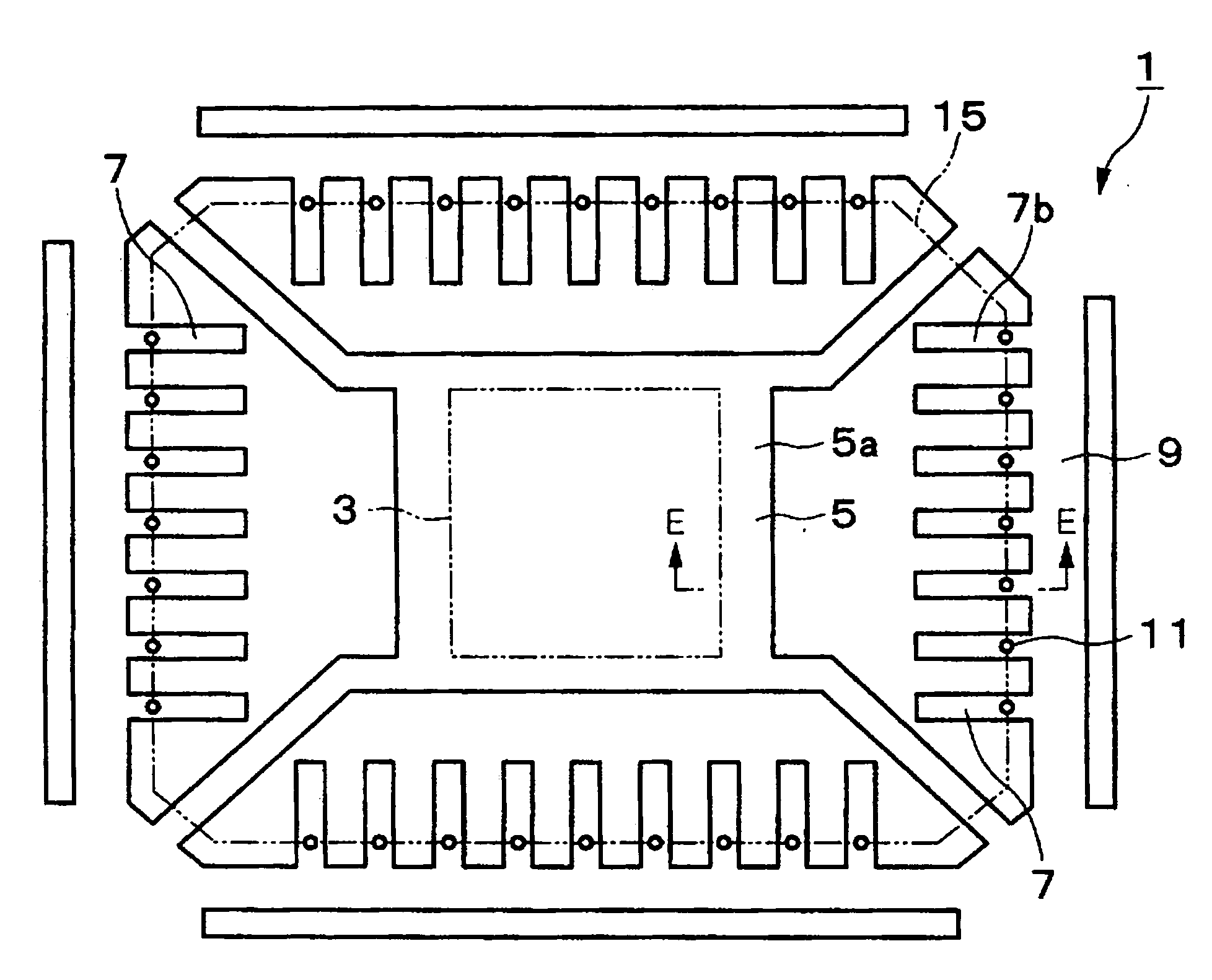
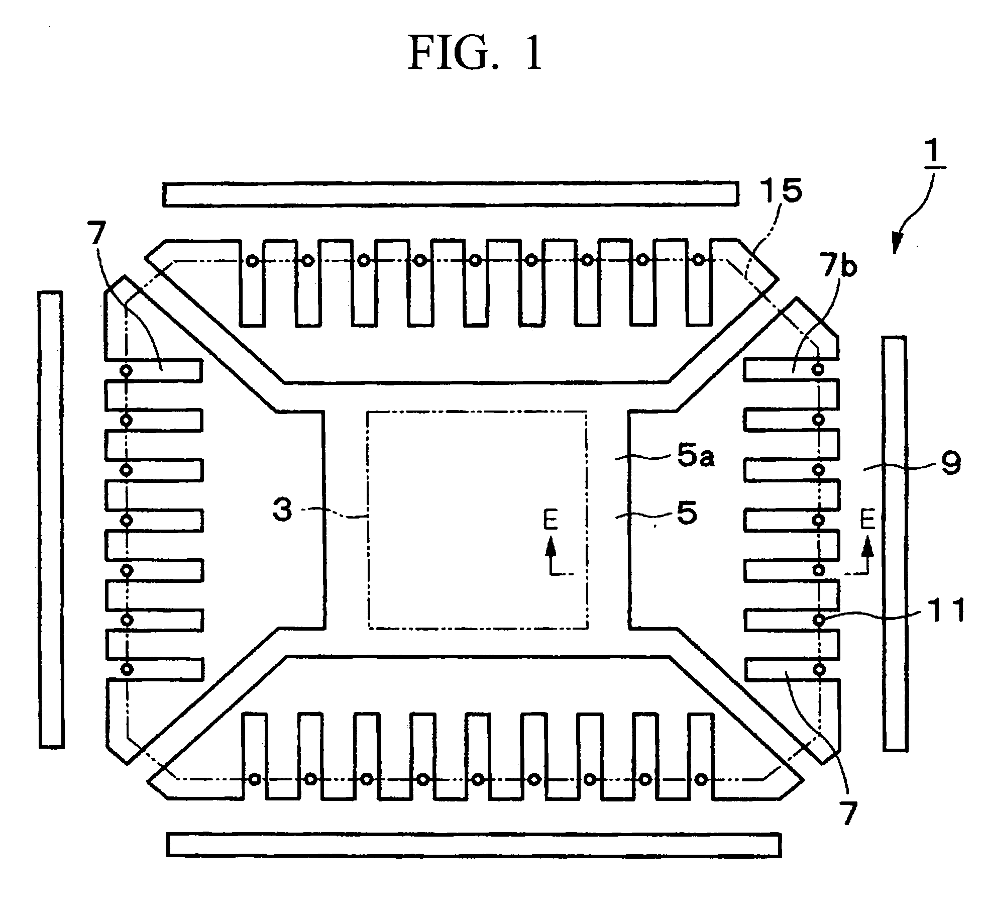
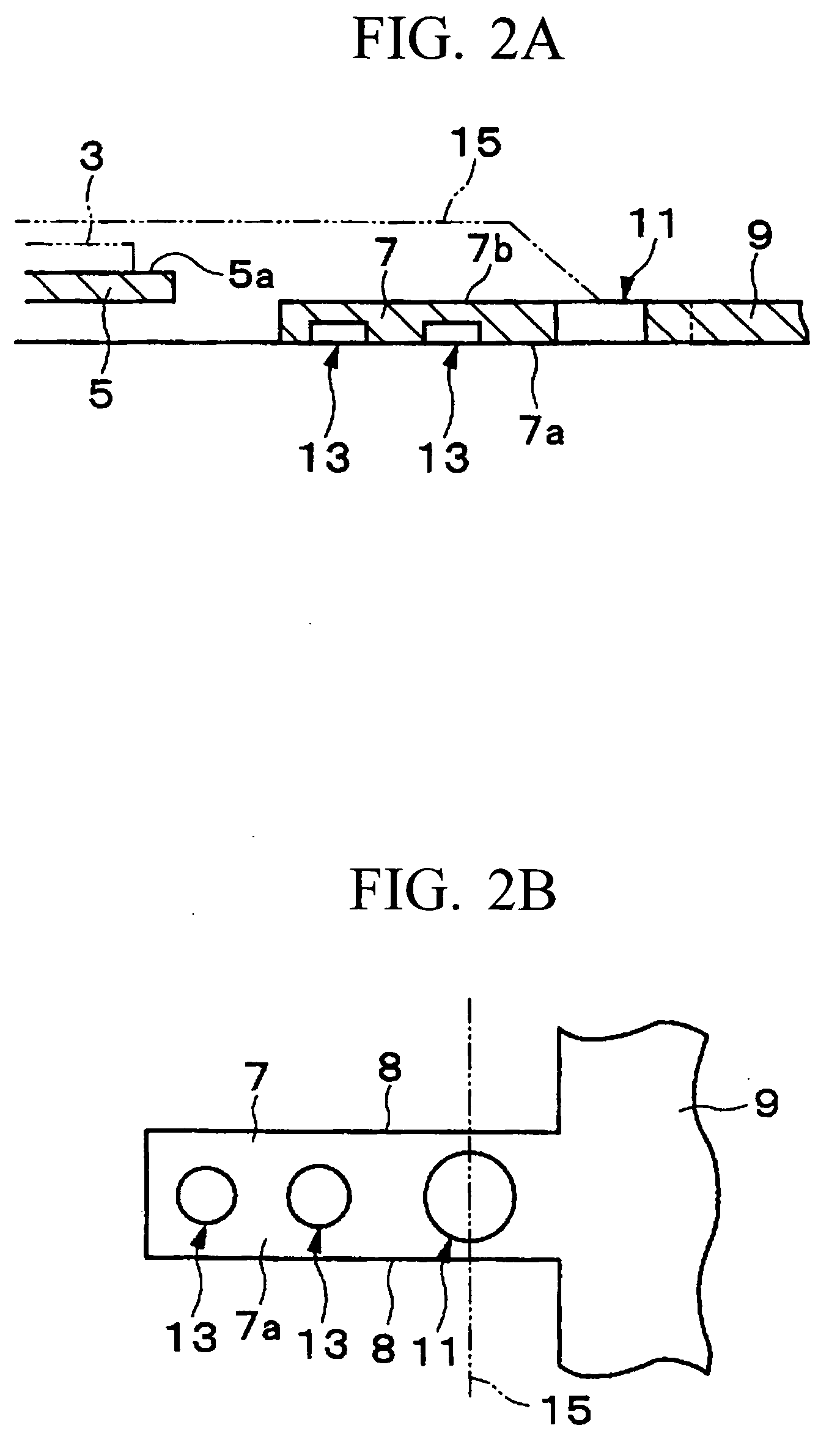
[0045]FIGS. 1, 2A, 2B, 3A, 3B, 4A, and 4B show essential parts of a semiconductor package in accordance with a preferred embodiment of the prevent invention. The semiconductor package of the first embodiment is produced using a lead frame that is formed by performing either press working or etching or both of them on a thin metal plate composed of copper.

[0046] Specifically, a lead frame 1 shown in FIG. 1 includes a stage 5 for mounting a semiconductor chip 3 thereon, plural leads 7 formed in the periphery of the stage 5, and dam bars (i.e., lead interconnecting members) 9 for interconnecting the leads 7 together.

[0047] The leads 7 have through holes 11, which run through the lead frame 1 in its thickness direction. The through holes 11 are formed to lie in an alignment direction of the leads 7. The through holes 11 are formed by press working or etching...


PUM


Abstract

A lead frame adapted to a semiconductor package, which is enclosed in a molded resin body and is connected with a board, is formed by processing a thin metal plate so as to include a stage for mounting a semiconductor chip thereon, a plurality of leads arranged to encompass the stage, and a plurality of lead interconnecting members (or dam bars) for interconnecting the leads together. At least one recess, which is of a circular shape or a non-circular shape, is formed on the backside of the lead (or the lead interconnecting member), which is substantially arranged in the same plane with a terminal surface of the molded resin body. Due to the formation of the recess that is subjected to plating, it is possible to increase the joining strength between the lead and solder; hence, it is possible to improve reliability regarding electric connection between the semiconductor package and board.

Description

BACKGROUND OF THE INVENTION [0001] 1. Field of the Invention [0002] The present invention relates to semiconductor packages encapsulating semiconductor chips connected to substrates and boards. The present invention also relates to lead frames for use in semiconductor packages. [0003] The present application claims priority on Japanese Patent Application No. 2004-372919, the content of which is incorporated herein by reference. [0004] 2. Description of the Related Art [0005] Conventionally, there are available a variety of semiconductor packages such as QFN (Quad Flat Non-Leaded) packages having plural leads partially exposed on terminal surfaces and side surfaces lying in thickness directions of molded resin bodies. An example of a conventionally-know semiconductor package is disclosed in Japanese Unexamined Patent Application Publication No. 2002-314024. FIG. 14 shows the layout of a lead frame 51 for use in a QFN package, which is produced using a lead frame 51 including a stage ...

Claims


Application Information

Patent Timeline
IPC IPC(8): H01L23/495H01L23/52
CPCH01L23/3107H01L23/49548H01L23/49582H01L24/48H01L2224/48091H01L2224/48247H01L2924/01078H01L2924/00014H01L2924/181H01L2924/00012H01L2224/45099H01L2224/45015H01L2924/207H01L23/495
Inventor SATO, TAKASHISHIRASAKA, KENICHI
Owner YAMAHA CORP
Why Eureka
Try Eureka