Flip-flop circuit

Active Publication Date: 2006-06-29
SEMICON COMPONENTS IND LLC
View PDF7 Cites 2 Cited by
  • Summary
  • Abstract
  • Description
  • Claims
  • Application Information

AI Technical Summary

Benefits of technology

[0010] The present invention has been proposed in order to solve the aforementioned problem, and an object of the present invention is

Problems solved by technology

In the exemplary conventional flip-flop circuit 101, therefore, the circuit

Method used


Image

  • Flip-flop circuit
  • Flip-flop circuit
  • Flip-flop circuit

Examples


first embodiment

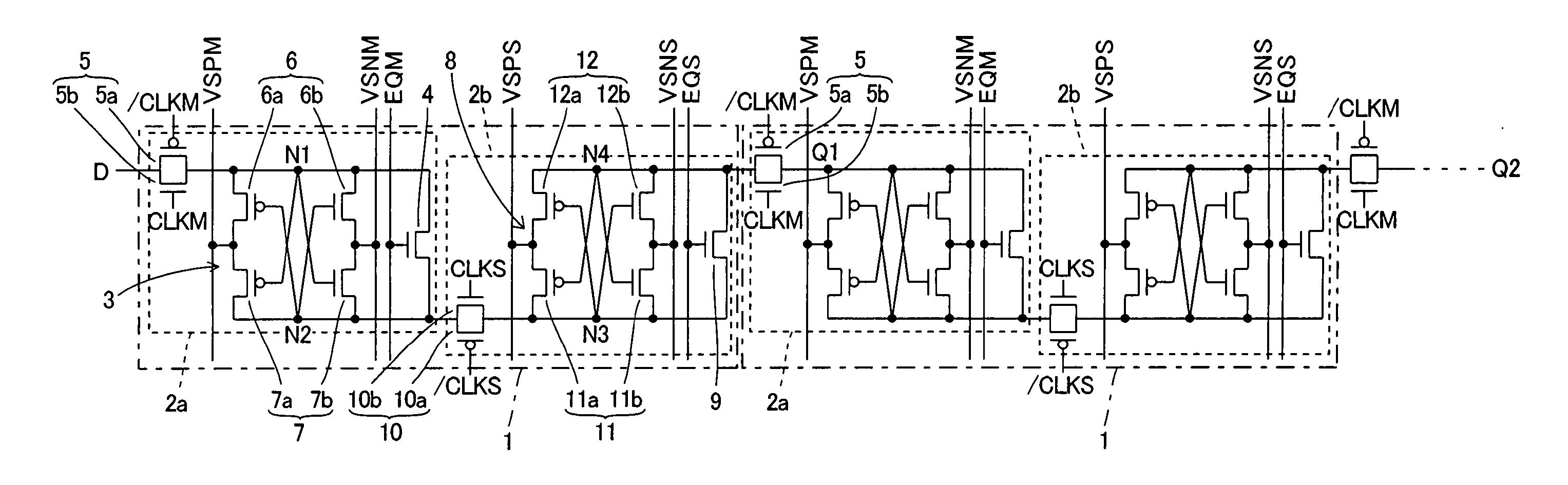
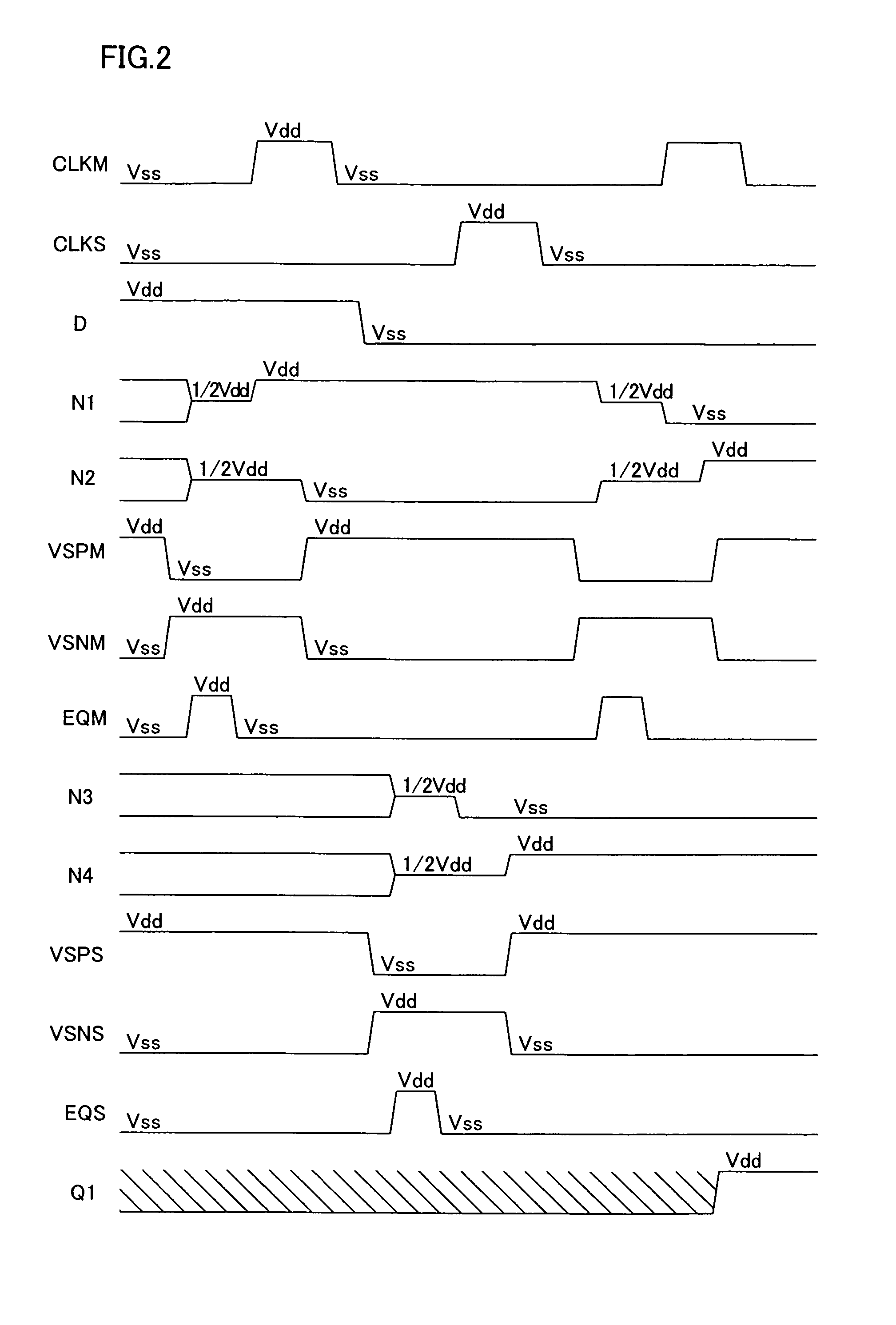
[0044] The circuit structure of a shift register circuit employing flip-flop circuits according to a first embodiment of the present invention is described with reference to FIG. 1.

[0045] As shown in FIG. 1, the shift register circuit is constituted of a plurality of stages of serially connected flip-flop circuits 1 according to the first embodiment. Each of the plurality of stages of flip-flop circuits 1 is constituted of two stages of delay latch circuits 2a and 2b. The delay latch circuits 2a and 2b are examples of the “first latch circuit” and the “second latch circuit” in the present invention respectively. The first-stage delay latch circuit 2a is formed to receive a prescribed input signal from a node D, latch the prescribed input signal for a constant period and thereafter output a signal obtained by inverting the potential of the prescribed input signal to the second-stage delay latch circuit 2b. The second-stage delay latch circuit 2b is formed to receive the output signa...

second embodiment

[0086] The structure of a DRAM employing a shift register circuit including flip-flop circuits according to a second embodiment of the present invention is now described with reference to FIG. 8.

[0087] As shown in FIG. 8, the DRAM according to the second embodiment includes memory cells 21 provided on positions where a word line WL and bit lines BL1 intersect with each other, a shift register circuit 22 and n-channel transistors 23a and 23b. Each memory cell 21 is constituted of an n-channel transistor 21a and a capacitor 21b. Either the source region or the drain region of the n-channel transistor 21a is connected to the corresponding bit line BL1, and either the drain region or the source region is connected to the capacitor 21. The gate of the n-channel transistor 21a is connected to the word line WL. The capacitor 21b holds charges responsive to data stored in the memory cell 21. In each of the n-channel transistors 23a and 23b, either the source region or the drain region is c...


PUM


Abstract

A flip-flop circuit capable of inhibiting current consumption as well as the circuit scale from increase is provided. This flip-flop circuit comprises a first latch circuit including first and second inverter circuits. A first power supply line capable of switching a supplied potential between a fixing potential supplied for fixing the potentials of output nodes of the first and second inverter circuits and a floating potential supplied for floating the potentials of the output nodes of the first and second inverter circuits is connected to the first latch circuit.

Description

BACKGROUND OF THE INVENTION [0001] 1. Field of the Invention [0002] The present invention relates to a flip-flop circuit, and more particularly, it relates to a flip-flop circuit including latch circuits. [0003] 2. Description of the Background Art [0004] A flip-flop circuit including various latch circuits is known in general. For example, Japanese Patent Laying-Open No. 8-279298 (1997) discloses such a flip-flop circuit. [0005]FIG. 11 shows an exemplary conventional flip-flop circuit 101 having a structure similar to that of the aforementioned flip-flop circuit disclosed in Japanese Patent Laying-Open No. 8-279298. As shown in FIG. 11, the exemplary conventional flop-flop circuit 101 is constituted of two delay latch circuits 102a and 102b and an inverter circuit 103. The first-stage delay latch circuit 102a is constituted of a latch circuit 104 and a transfer gate transistor 105. The latch circuit 104 is constituted of two inverter circuits 106 and 107 and a transfer gate transis...

Claims


Application Information

Patent Timeline
IPC IPC(8): H03K3/037
CPCG11C19/00G11C19/28H03K3/012H03K3/0372
Inventor MIYAMOTO, HIDEAKI
Owner SEMICON COMPONENTS IND LLC
Why Eureka
Try Eureka