Optical element, lithographic apparatus including such an optical element, device manufacturing method, and device manufactured thereby

Active Publication Date: 2006-07-06
ASML NETHERLANDS BV
View PDF40 Cites 31 Cited by
  • Summary
  • Abstract
  • Description
  • Claims
  • Application Information

AI Technical Summary

Benefits of technology

[0019] As the EUV radiation may be reflected from the anti-reflection coating, a substrate underneath may be designed to improve the anti-reflection properties of the optical element. The substrate may be made from any suitable metal or alloy which has good heat conductivity. The substrate may be made from silicon or copper. The substrate may absorb the light that is being suppressed which helps to prevent transmitted light from entering the lithography apparatus. Moreover, the substrate may have a low thermal expansion coefficient.
[0020] To broaden the suppression of unwanted radiation such as DUV and IR, a coating material may be used which has a low natural grazing incidence reflectivity at other wavelengths, for example in the UV range. For example, the substrate may have a coating of diamond of about 40 mm thickness. The diamond has l

Problems solved by technology

This non-EUV radiation may be harmful for the EUV lithography system, so it should be removed by a spectral purity filter.

Method used


Image

  • Optical element, lithographic apparatus including such an optical element, device manufacturing method, and device manufactured thereby
  • Optical element, lithographic apparatus including such an optical element, device manufacturing method, and device manufactured thereby
  • Optical element, lithographic apparatus including such an optical element, device manufacturing method, and device manufactured thereby

Examples


Example

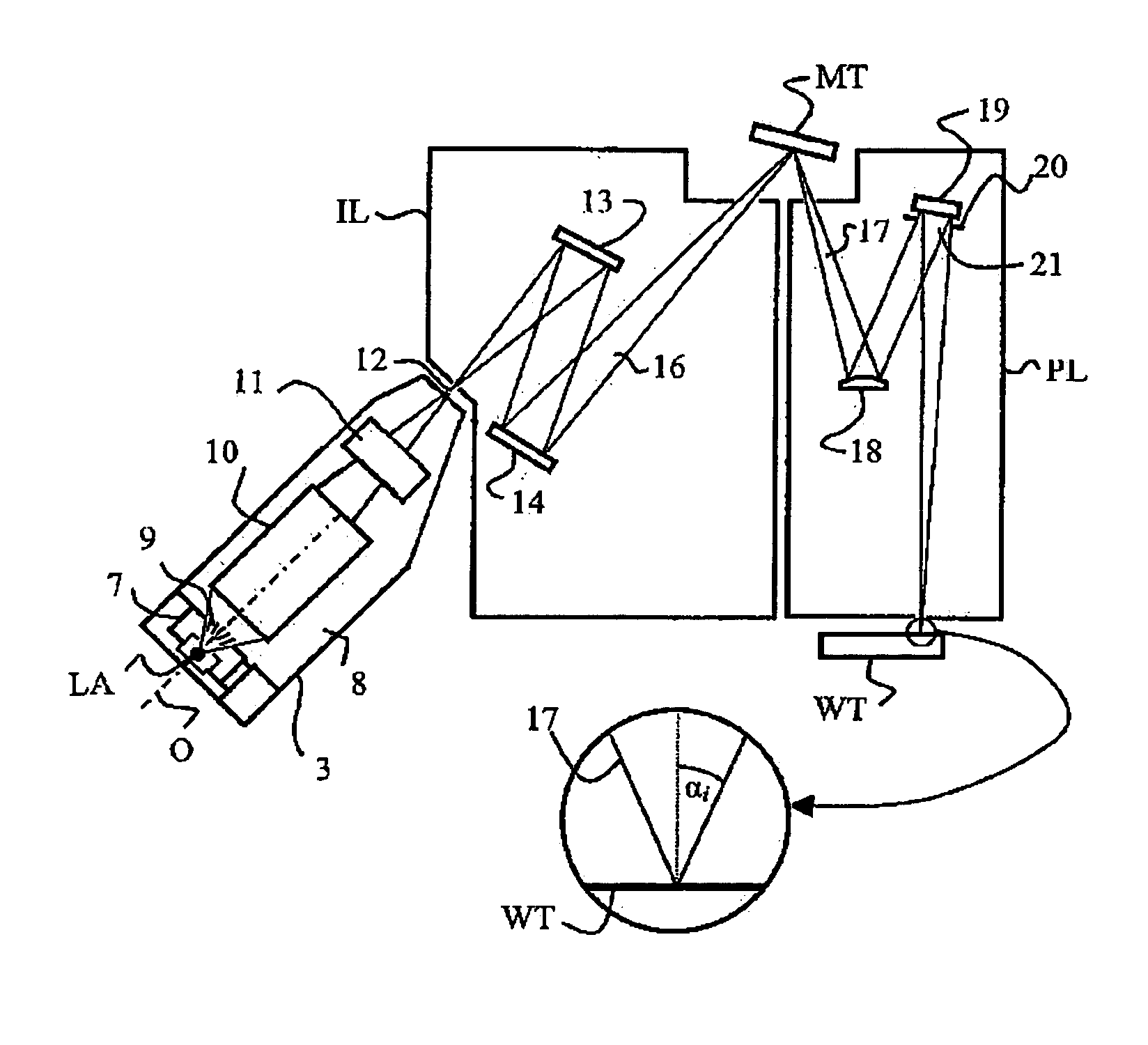
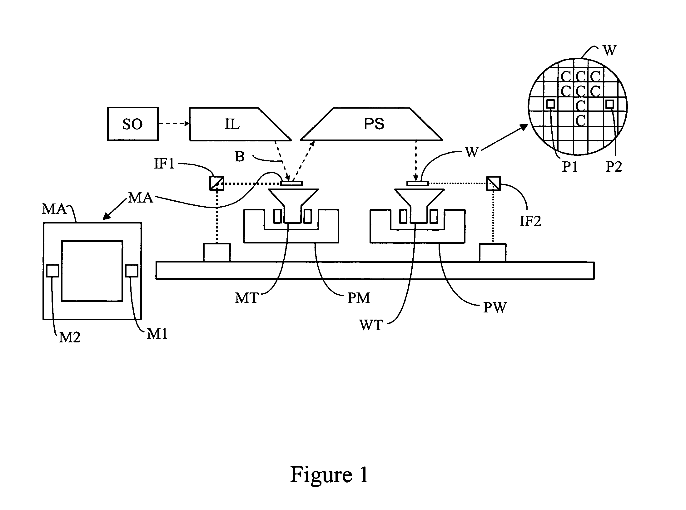
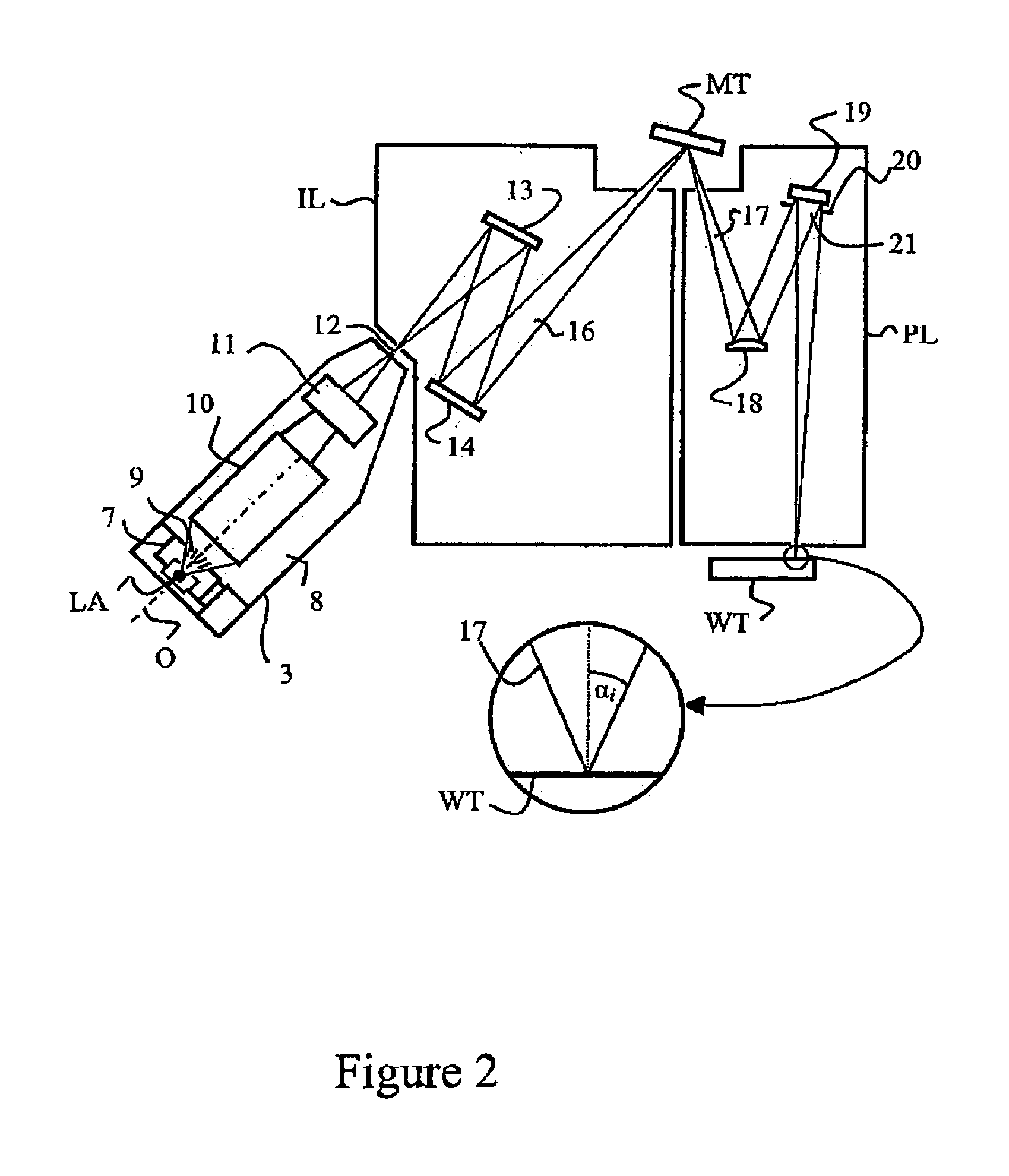
[0041]FIG. 1 schematically depicts a lithographic apparatus according to one embodiment of the invention. The apparatus includes an illumination system (illuminator) IL configured to condition a radiation beam B (e.g. UV radiation or EW radiation). A support (e.g. a mask table) MT is configured to support a patterning device (e.g. a mask) MA and is connected to a first positioning device PM configured to accurately position the patterning device in accordance with certain parameters. A substrate table (e.g. a wafer table) WT is configured to hold a substrate (e.g. a resist-coated wafer) W and is connected to a second positioning device PW configured to accurately position the substrate in accordance with certain parameters. A projection system (e.g. a refractive projection lens system) PS is configured to project a pattern imparted to the radiation beam B by patterning device MA onto a target portion C (e.g. including one or more dies) of the substrate W.

[0042] The illumination sys...


PUM


Abstract

An optical element including an anti-reflection (AR) coating is configured to reflect Extreme-Ultra-Violet (EUV) radiation only.

Description

BACKGROUND OF THE INVENTION [0001] 1. Field of the Invention [0002] The present invention relates to an optical element, a lithographic apparatus including such an optical element, a device manufacturing method, and a device manufactured thereby. [0003] 2. Description of the Related Art [0004] A lithographic apparatus is a machine that applies a desired pattern onto a substrate, usually onto a target portion of the substrate. A lithographic apparatus can be used, for example, in the manufacture of integrated circuits (ICs). In that instance, a patterning device, which is alternatively referred to as a mask or a reticle, may be used to generate a circuit pattern to be formed on an individual layer of the IC. This pattern can be transferred onto a target portion (e.g. including part of, one, or several dies) on a substrate (e.g. a silicon wafer). Transfer of the pattern is typically via imaging onto a layer of radiation-sensitive material (resist) provided on the substrate. In general...

Claims


Application Information

Patent Timeline
IPC IPC(8): G03F7/20
CPCG03F7/70575G03F7/70958G21K1/06G21K2201/067G02B1/113G02B5/0891
Inventor WILHELMUS VAN HERPEN, MAARTEN MARINUS JOHANNESBAKKER, LEVINUS PIETERWILFRED KLUNDER, DERK JAN
Owner ASML NETHERLANDS BV
Why Eureka
Try Eureka