IC tag and IC tag attachment structure

a technology of ic tags and attachment structures, applied in the field of ic tags, can solve the problems of metal objects, inability to use antennas with spacers, and tend to degrade the characteristics of antennas, and achieve the effect of wide directivity in free spa

Inactive Publication Date: 2006-07-06
DENSO CORP
View PDF1 Cites 179 Cited by
  • Summary
  • Abstract
  • Description
  • Claims
  • Application Information

AI Technical Summary

Benefits of technology

[0015] The antenna for the IC tag used for the RFID is required to: (1) have wide directivity in free space; (2) function near a metal (this naturally ensures functioning near a dielectric material); (3) achieve the impedance matching with the IC chip; and (3) be thin.
[0021] In addition, in the IC tag of the present invention, the IC chip is surface-mounted and connected with the first transmission metal plate through the matching metal plate. Therefore, the impedance matching between the IC chip and the antenna can be achieved.
[0023] Thus, the antenna in the IC tag of the present invention has wide directivity in free space, functions near a metal or a dielectric material, achieves the impedance matching with the IC chip, and can be designed to be thin.

Problems solved by technology

The object, especially the metal object, tends to degrade the characteristics of the antennas.
However, as for the UHF (960 MHz) frequency range, the antenna with the spacer is not practical because λ / 4 roughly equals no less than 8 cm.

Method used


Image

  • IC tag and IC tag attachment structure
  • IC tag and IC tag attachment structure
  • IC tag and IC tag attachment structure

Examples


first embodiment

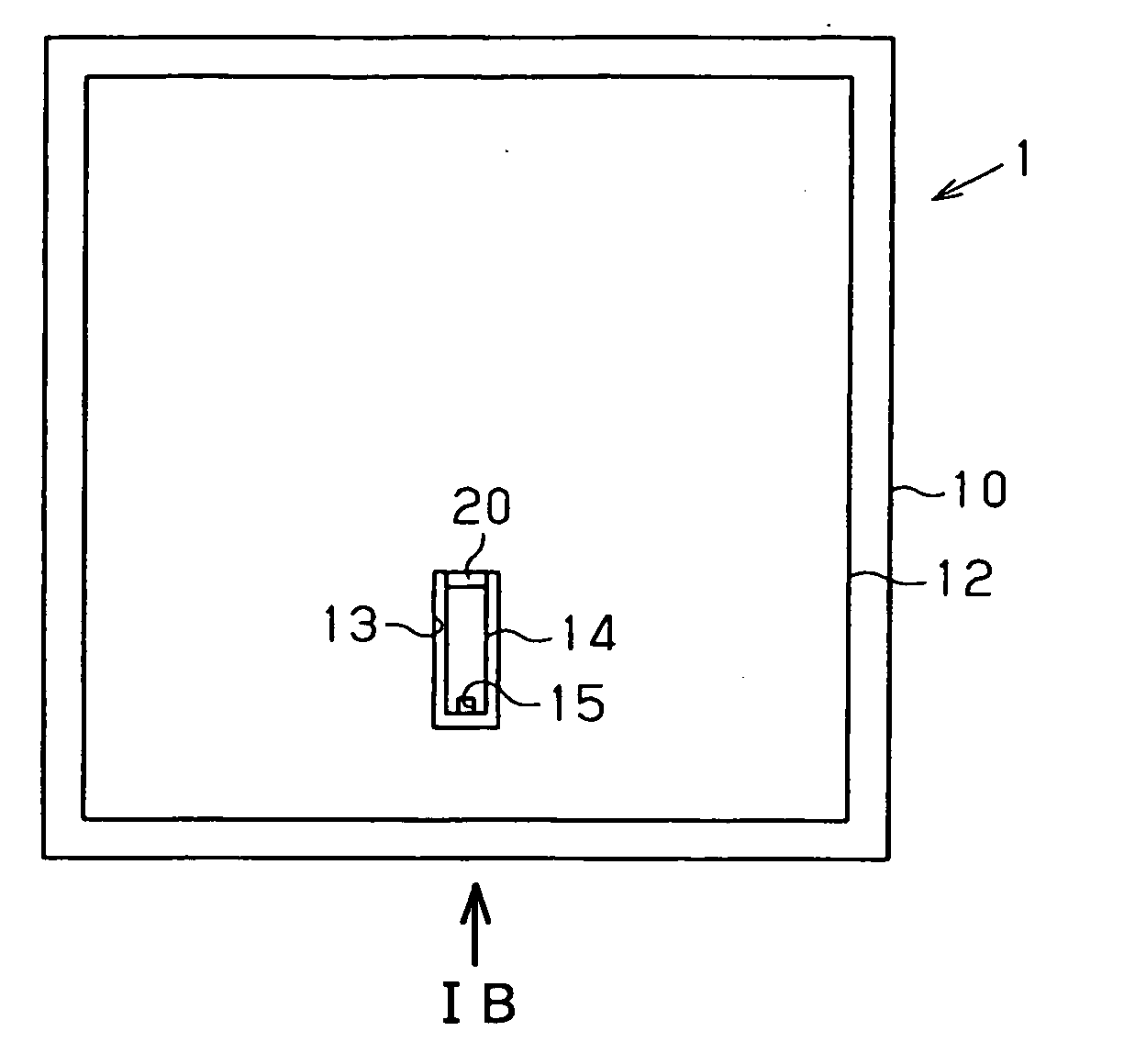
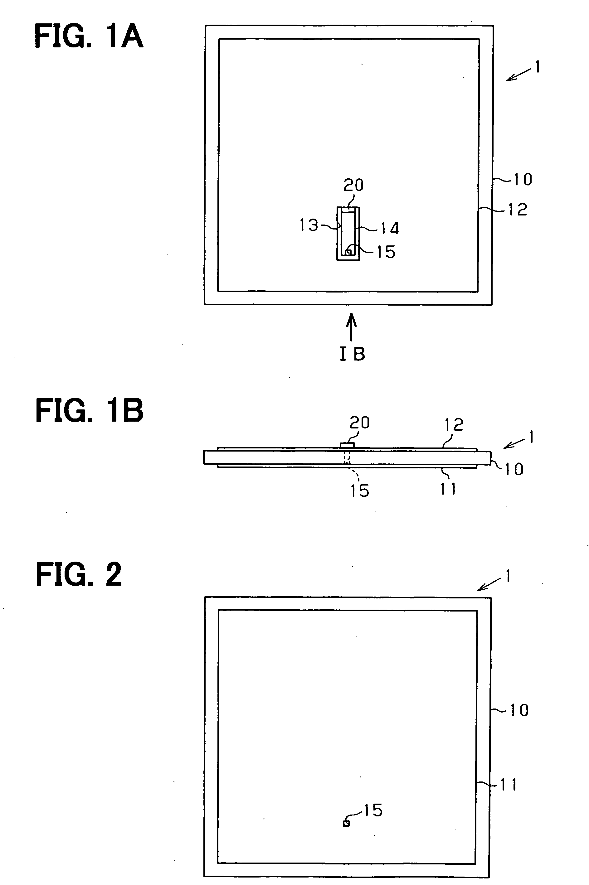
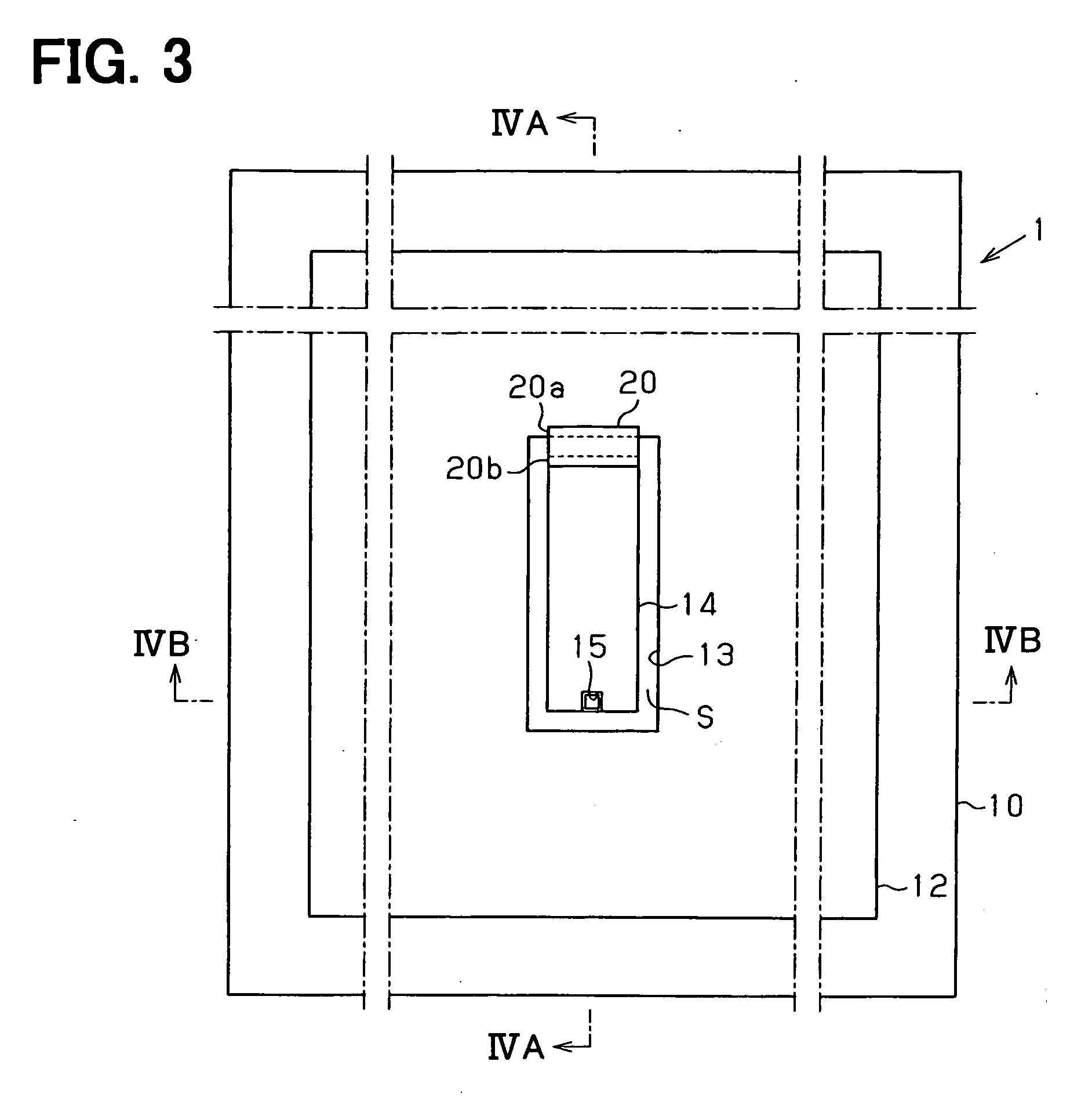
[0051] Hereafter, a first embodiment of the present invention is described with reference to FIGS. 1A-4B. As shown in FIGS. 1A, 1B and 2, an IC tag 1 of the first embodiment includes a dielectric body 10 of a plate shape, which is square and planar. A first metal plate 11 for transmission is fixed to a bottom surface of the dielectric body 10 having a square planar shape.

[0052] A second metal plate 12 for transmission is fixed to an upper surface of the dielectric body 10 with its outer edge (or peripheral edge) nearly (or substantially) facing symmetrically with (or overlapping with) an outer edge of the first metal plate 11 via the dielectric body 10. Therefore, an area surrounded by the outer edge of the second metal plate 12 has nearly (or substantially) the same size as an area surrounded by the outer edge of the first metal plate 11 has. The second metal plate 12 has a hole 13 of an oblong (or rectangular) shape. The metal plates 11 and 12 together constitute an antenna.

[005...

second embodiment

[0080] The IC tag 1 of a second embodiment differs from the first embodiment in that, as shown in FIGS. 13A and 13B, the first metal plate 11 and second metal plate 12 are fixed to the dielectric body 10, within a given misalignment ΔY. This given misalignment ΔY is λ / 30 measured in a direction along the surfaces of the dielectric body 10 between the outer edge of the first metal plate 11 and the outer edge of the second metal plate 12. Here, the value λ is wavelength of an electric wave in the dielectric body 10.

[0081] Specifically, in FIGS. 13A, 13B, the outer edge of the second metal plate 12 is slightly smaller than that of the first metal plate 11 with the misalignment ΔY within λ / 30. Alternatively, the outer edge of the second metal plate 12 may be slightly larger than that of the first metal plate 11 also with the misalignment ΔY within λ / 30.

[0082] In FIGS. 13C, 13D, the outer edge of the second metal plate 12 is as large as the outer edge of the first metal plate 11 with t...


PUM

PropertyMeasurementUnit
microwave frequencyaaaaaaaaaa
impedanceaaaaaaaaaa

Abstract

A first metal plate for transmission and a second metal plate for transmission are closely-attached to a first surface and a second surface of a dielectric body, respectively. An outer edge of the first metal plate substantially symmetrically faces an outer edge of the second metal plate via the dielectric body. A metal plate for matching is arranged inside a hole formed on the second metal plate, with a slit formed with an inner wall of the hole, and is fixed to the dielectric body. The metal plate for matching is electrically connected to the first metal plate via a through hole penetrating the dielectric body. An IC chip is surface-mounted to connect the second metal plate with the metal plate for matching.

Description

CROSS REFERENCE TO RELATED APPLICATION [0001] This application is based on and incorporates herein by reference Japanese patent application No. 2004-364581 filed on Dec. 16, 2004. FIELD OF THE INVENTION [0002] The present invention relates to an IC tag used for RFID (Radio Frequency IDentification) and utilizing a microwave frequency range in wireless communications, and in particular to an art for constructing a system which is capable of providing steady data exchange wherever it is installed. For example, the system is installed on a dielectric material or a metal. BACKGROUND OF THE INVENTION [0003] RFID is an auto-recognition system for reading / writing (specifically, retrieving, registering, deleting, or updating) individual information from / to a person or a substance memorized in a medium called an IC tag by using wireless communications. FIG. 18 is a schematic view showing an example of the system. [0004] Two devices are necessary in order to provide the RFID. One is a reader / ...

Claims


Application Information

Patent Timeline
Patent Type & Authority Applications(United States)
IPC IPC(8): G08B13/14G06K19/06H01L23/02
CPCG06K19/07749G06K19/07771H01L23/49855H01L2924/0002H01L2924/00G06K19/077H04B5/02G06K19/07
Inventor TANAKA, MAKOTOMATSUGATANI, KAZUOKIKIM, MOONILKIM, WON HO
Owner DENSO CORP
Why Eureka
Try Eureka