Semiconductor memory

a memory and semiconductor technology, applied in the field of semiconductor memory, can solve problems such as erroneous operation of sense amplifiers, and achieve the effects of preventing scattering in bit line potentials during read operations, reducing potential differences, and increasing the potential of reference bits

Active Publication Date: 2006-07-06
FUJITSU SEMICON MEMORY SOLUTION LTD +1
View PDF2 Cites 12 Cited by
  • Summary
  • Abstract
  • Description
  • Claims
  • Application Information

AI Technical Summary

Benefits of technology

[0012] When a normal memory cell is selected, different charges flow in the normal bit line according to the state of the storage capacitor of the normal memory cell, changing the potential of the bit line to a different level. In the storage capacitor of the reference memory cell is stored data causing a large amount of charge to flow to the reference bit line; when a normal memory cell is selected, the reference memory cell is also selected, and the potential of the reference bit line is made higher. Due to the current mirror circuit, the potential of the reference bit line is held at a level higher by the threshold voltage thereof than the source potential of the first transistor, the potential of a normal bit line of a normal memory cell storing the same data as the reference memory cell is held at the same level as the reference bit line, and the potential of a normal bit line of a normal memory cell storing data different from that of the reference memory cell is held at the source potential of the second transistor. Hence the potential of a normal bit line is reliably held at either a first level equal to the source potential, or at a second level higher than the source potential by the threshold voltage thereof. Thus even though the capacitance values of ferroelectric capacitors is scattered, the scattering in the bit line potentials during read operations can be prevented.
[0013] In the above first aspect, it is preferable that a preamp circuit, which amplifies the potential of a normal bit line based on the potential of the normal bit line and the potential of the reference bit line, is provided for each normal bit line. This preamp circuit compares a first level generated by the normal bit line, and a second level potential higher than the first level by a threshold voltage with the potential of the reference bit line, and performs amplification to the higher potential difference. If the source potentials of the first transistor and of the second transistor are the same, the potential of the reference bit line is always held at the second level, so that the amplification operation of the preamp circuit is performed more reliably.

Problems solved by technology

However, the capacitance values of ferroelectric capacitors formed from ferroelectric material is scattered considerably due to the manufacturing process used therefor, and consequently there is also scattering in the bit line potential during reading, causing erroneous operation of the sense amplifier.

Method used


Image

  • Semiconductor memory
  • Semiconductor memory
  • Semiconductor memory

Examples


Embodiment Construction

[0021] Below, embodiments of the invention are explained referring to the drawings. However, the technical scope of the invention is not limited to these embodiments, but extends to the inventions described in the scope of claims and to inventions equivalent thereto.

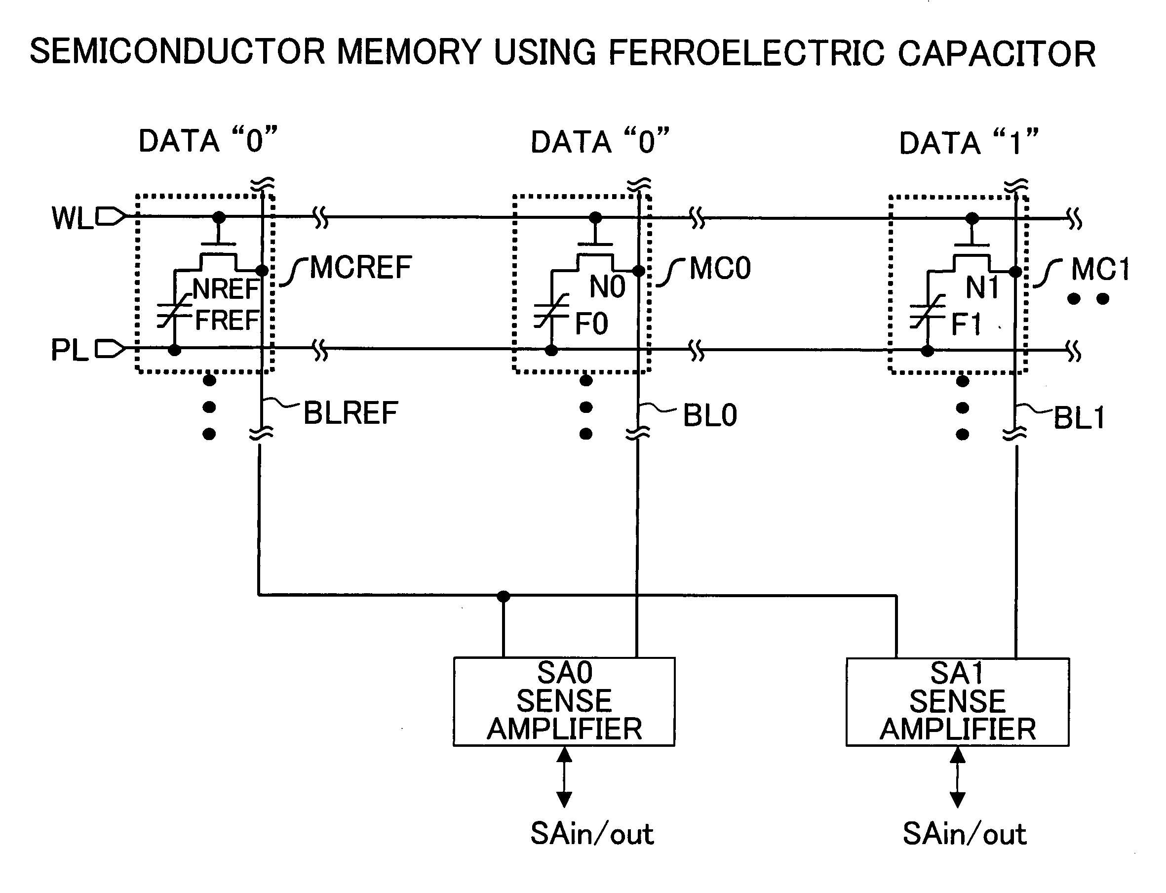
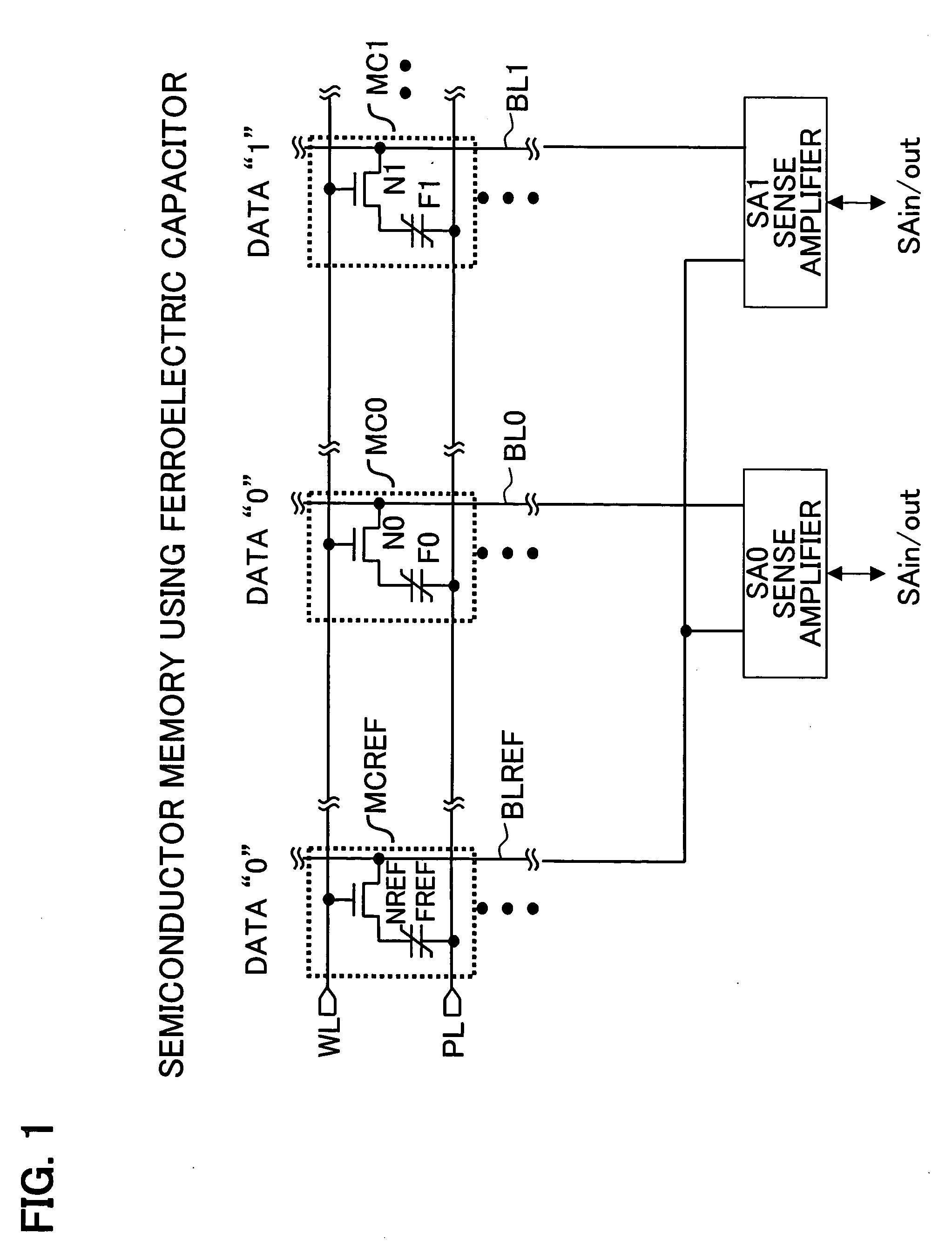
[0022] Prior to explaining the embodiments, semiconductor memory using ferroelectric capacitors is explained. The following example is for ferroelectric memory with one-transistor, one-capacitor type memory cells.

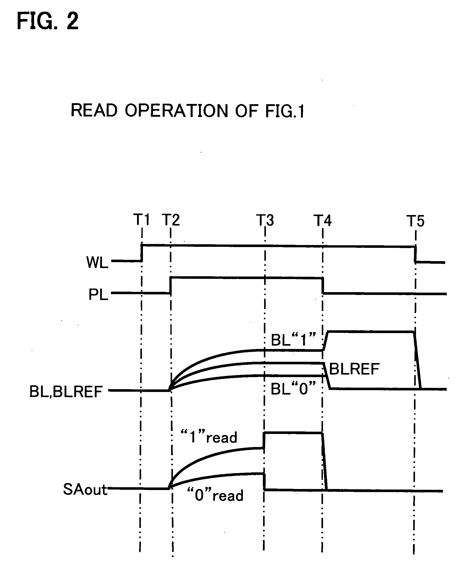
[0023]FIG. 1 shows the configuration of semiconductor memory using ferroelectric capacitors. In FIG. 1 are shown one word line WL, one plate line PL, two normal bit lines BL0 and BL1, one reference bit line BLREF, two normal memory cells MC0 and MC1, and one reference memory cell MCREF. Each of the memory cells MC0, MC1, MCREF has a cell transistor N0, N1, NREF the gate of which is connected to the word line and the terminal of the source or drain of which is connected to a bit line BL0, BL1, BLREF, and a ferr...


PUM


Abstract

The semiconductor memory has word lines; normal memory cells each having a storage capacitor; normal bit lines connected to the normal memory cells; a reference memory cell having a capacitor storing prescribed data; and a reference bit line connected to the reference memory cell. When a word line is selected, the potential of normal bit lines and of reference bit line changes according to the charge on the storage capacitors and on the reference capacitor. A current mirror circuit is also provided, which has a first transistor drain of which is connected to the reference bit line and second transistors drains of which are respectively connected to normal bit lines, the gates of the first and second transistors being connected in common to the reference bit line. Thus even though the capacitance values of ferroelectric capacitors is scattered, the scattering in bit line potentials during read operations can be prevented.

Description

CROSS-REFERENCE TO RELATED APPLICATIONS [0001] This application is based upon and claims the benefit of priority from the prior Japanese Patent Application No. 2005-555, filed in Jan. 5, 2005, the entire contents of which are incorporated herein by reference. BACKGROUND OF THE INVENTION [0002] 1. Field of the Invention [0003] This invention relates to a semiconductor memory, and in particular relates to a read circuit for nonvolatile memory using a ferroelectric memory device. [0004] 2. Description of the Related Art [0005] Ferroelectric memory (FeRAM) is a memory which uses ferroelectric capacitors as memory cells, and is a nonvolatile memory which can retain stored information even when the power supply is turned off. Similarly to SRAM and other memory types, ferroelectric memory can write and read data rapidly and with low power consumption. For these reasons, ferroelectric memory is used widely in IC cards, game equipment, tag chips, and other storage media. Such ferroelectric m...

Claims


Application Information

Patent Timeline
Patent Type & Authority Applications(United States)
IPC IPC(8): G11C7/02G11C7/14G11C11/22
CPCG11C11/22G11C5/063G11C7/06G11C7/18G11C8/14G11C11/221G11C11/2273
Inventor MORITA, KEIZO
Owner FUJITSU SEMICON MEMORY SOLUTION LTD
Why Eureka
Try Eureka