Shift register and method for driving the same
a technology of shift register and drive circuit, which is applied in the direction of digital storage, counting chain synchronous pulse counters, instruments, etc., can solve the problems of constant deterioration increased voltage of thin film transistors, and worse mobility
- Summary
- Abstract
- Description
- Claims
- Application Information
AI Technical Summary
Benefits of technology
Problems solved by technology
Method used
Image
Examples
first embodiment
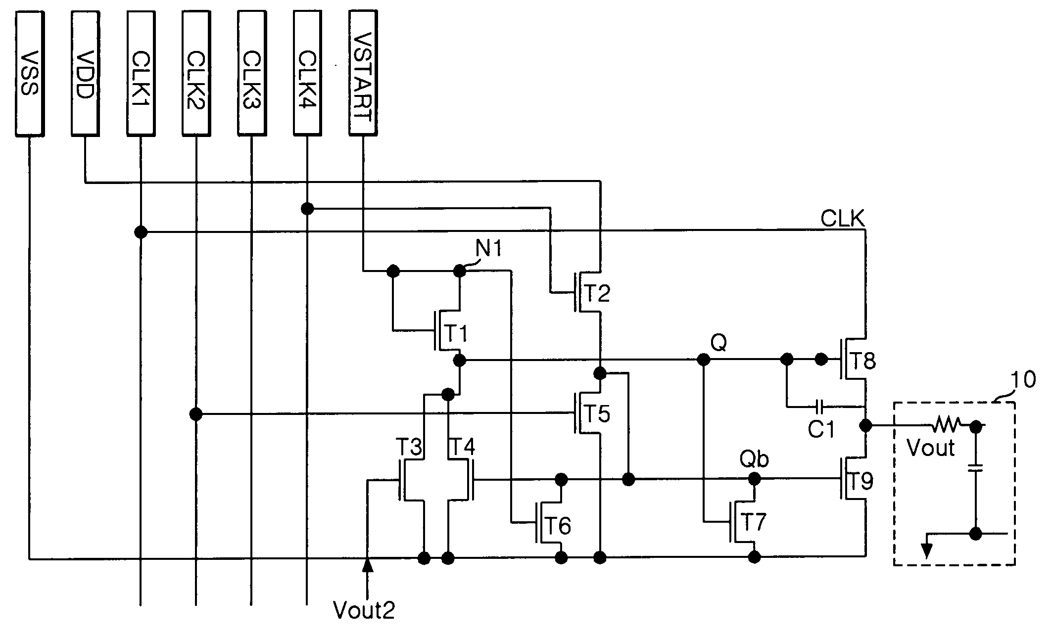
[0068]FIG. 7 is a diagram representing a drive waveform for driving a shift register of FIGS. 5 and 6 and an output waveform in accordance therewith. A driving method of the shift register according to the present invention will be explained by FIG. 7 in conjunction with FIGS. 5 and 6.
[0069] In a T1 period, the start pulse or the previous stage's output signal is inputted in synchronization with the fourth clock signal CLK4. If the start pulse Vstart is inputted, the first NMOS transistor T1 is turned on and the Q node is charged with as much voltage as the start pulse Vstart. At the same time, if the fourth clock signal CLK4 is inputted, the second NMOS transistor T2 is turned on and the Qb node is charged with the voltage from the second voltage supply source VDD. However, the sixth NMOS transistor T6 is turned on by the start pulse Vstart and the seventh NMOS transistor T7 is turned on by the voltage charged in the Q node, thus the voltage charged in the Qb node is discharged thr...
second embodiment
[0125] Hereinafter, the operation of the shift register of the T2 period to the T8 period is the same as the foregoing second embodiment, thus the detail explanation on this will be omitted.
[0126] It is desirable that the period when the logic value of the Qb node is in the high state and while the logic value of the output signal line is low includes a clock signal when the output signal of the pertinent stage is generated, e.g., the period when the first clock signal is inputted in the first stage.
[0127] The present invention can reduce the accumulated voltage stress which is generated by a continuous voltage application to the Qb node. Further, the shift register and driving method thereof of the present invention can be driven by a two-phase, three-phase or five-phase clock.
[0128]FIG. 11 is a diagram briefly representing the configuration of the shift register of the present invention, and represents an example of using a two phase clock in a simple circuit.
[0129] Referring t...
PUM
 Abstract
Description
Claims
Application Information


