
Integrated MEMS packaging

a technology of integrated mems and packaging, which is applied in the manufacture of microstructural devices, electrical apparatus, and semiconductor devices, etc., can solve the problems of large impact, noise inherent in the electrical connection between the mems package and the rest of the system, and large packaging proportion of the total cost of the mems device, so as to improve the overall electrical quality of the system

Active Publication Date: 2006-07-06
SHARP KK
View PDF3 Cites 51 Cited by
  • Summary
  • Abstract
  • Description
  • Claims
  • Application Information

AI Technical Summary

Benefits of technology

This patent describes a low-cost packaging system for integrating electrical, mechanical, and optical MEMS devices with electrical systems. The invention allows for the integration of MEMS devices on glass substrates using low temperature polysilicon technology, resulting in better overall system electrical quality. The method involves forming an electrical circuit on a first substrate, integrating the MEMS device on a first substrate region, providing a second substrate overlying the first substrate, and forming a wall along the first region boundaries to enclose the MEMS device. The wall can act to isolate the MEMS device from the electrical circuit while exposing it to an environment. The invention has applications in various fields such as cell phones, sensors, and actuators.

Problems solved by technology

One problem with this type of MEMS packaging methodology is that the package is a very large proportion of the total MEMS device cost; on the order of 30-70% of the overall cost.
This packaging cost can, therefore, have a significant impact on the capability of such MEMS devices to penetrate cost-sensitive markets, such as the cell phone market.
Another problem with existing MEMS packaging is the noise inherent with the electrical connections between the MEMS package and the rest of the system.
The bonding, wiring, and electrical interconnections associated with interfacing a MEMS device embedded in a package, to a circuit, necessarily adds impedance mismatches that result in noisy or low amplitude signals.
The issues preventing MEMS penetration into the cell phone market are cost and performance.
This cost issue is preventing the integration of MEMS into cell phones, display systems, and many other types of electronic devices.
The integration of MEMS into larger scale systems has been expensive to fabricate due to the process difficulties and the cost associated with integrating the MEMS standard IC technologies, such as CMOS.

Method used


Image

  • Integrated MEMS packaging
  • Integrated MEMS packaging
  • Integrated MEMS packaging

Examples


Embodiment Construction

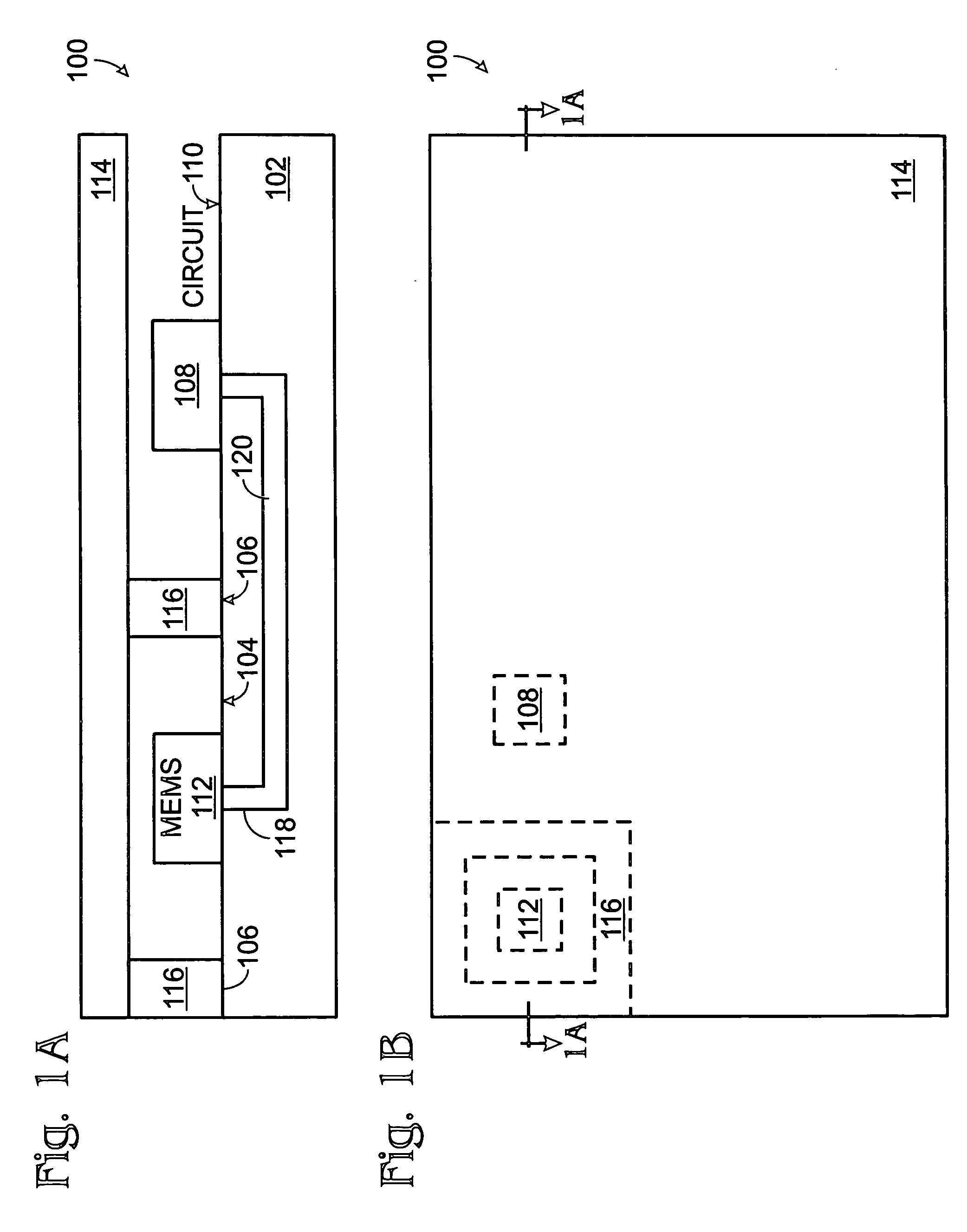
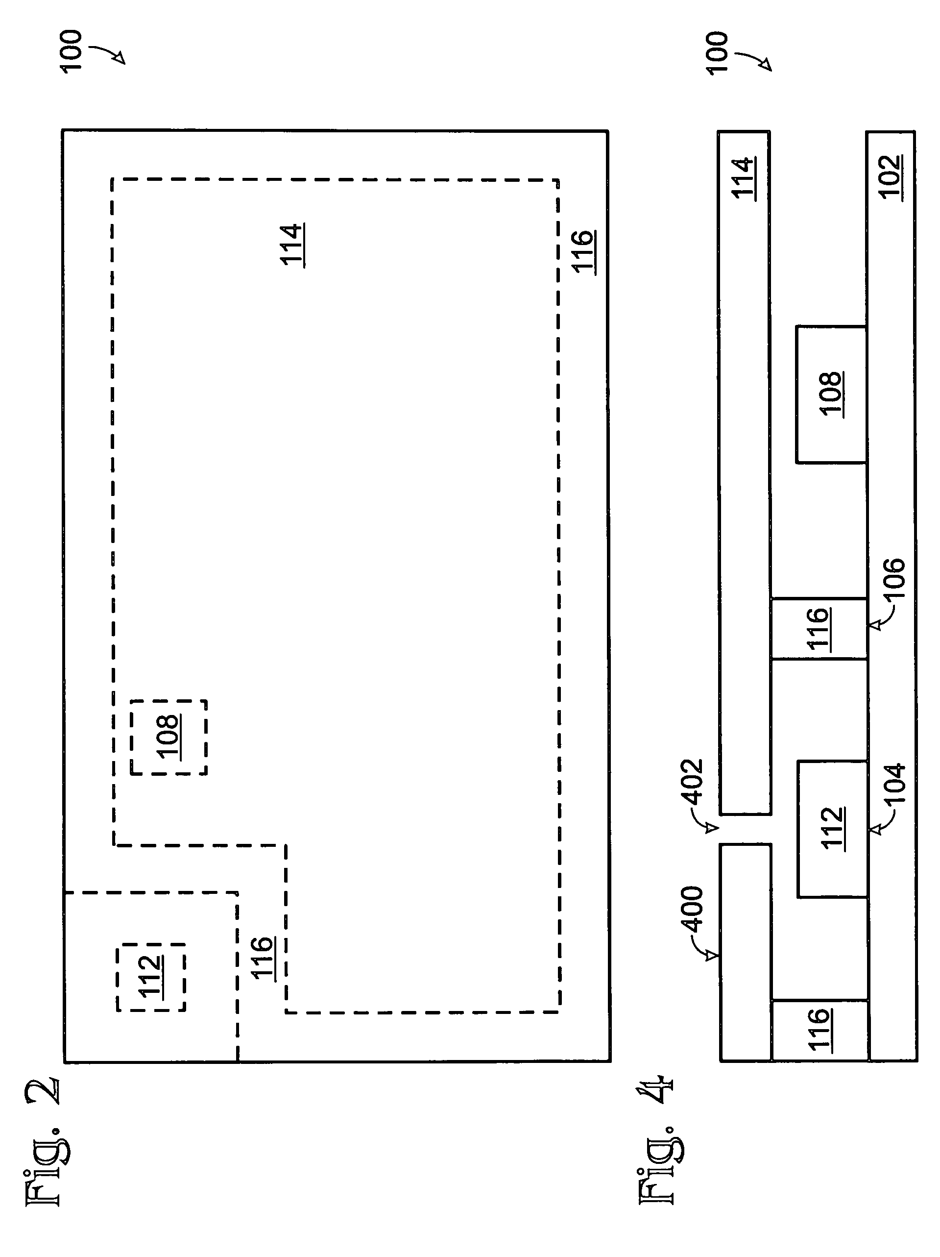
[0039]FIGS. 1A and 1B is a partial cross-sectional and plan views, respectively, of an integrated microelectromechanical system (MEMS) device package. The MEMS integrated package 100 comprises a first substrate 102 having a first region 104 with boundaries 106. An electrical circuit 108 is formed on a second region 110 of the first substrate 102. The electrical circuit 108 is electrically connected to the first substrate 102. For example, traces in the first substrate may conduct dc power, ground, and electrical signals to the electrical circuit 108. A MEMS device 112 is shown on the first region 104, electrically connected to the first substrate 102. The boundaries 105 may, or may not completely form a perimeter that surrounds the MEMS device 112. A second substrate 114 overlies the first substrate 102. A wall 116 is formed along the first region boundaries 106, between the first substrate 102 and second substrate 114.

[0040] In its simplest form, the first substrate 102 is a one-s...


PUM


Abstract

An integrated MEMS package and associated packaging method are provided. The method includes: forming an electrical circuit, electrically connected to the first substrate; integrating a MEMS device on a first substrate region, electrically connected to the first substrate; providing a second substrate overlying the first substrate; and, forming a wall along the first region boundaries, between the first and second substrate. In one aspect, the electrical circuit is formed using thin-film processes; and, wherein integrating the MEMS device on the first substrate region includes forming the MEMS using thin-film processes, simultaneous with the formation of the electrical device. Alternately, the MEMS device is formed in a separate process, attached to the first substrate, and electrical interconnections are formed to the first substrate using thin-film processes.

Description

RELATED APPLICATIONS [0001] This application is a continuation-in-part of a pending patent application entitled, PIEZO-TFT CANTILEVER MEMS, invented by Zhan et al., Ser. No. 11 / 031,320, filed 01 May 2005. This application is incorporated herein by reference.BACKGROUND OF THE INVENTION [0002] 1. Field of the Invention [0003] This invention generally relates to the packaging of microelectromechanical systems (MEMS) and, more particularly, to a system and method for simultaneously packaging a MEMS device with active circuitry on an integrated circuit (IC) substrate. [0004] 2. Description of the Related Art [0005] MEMS devices are typically made on silicon wafers; using one of two well established techniques: bulk micro-machining or surface micro-machining. In both of these methods, the MEMS device is fabricated on a silicon wafer using standard IC-type fabrication equipment. Once the wafer is processed, the wafer is diced to form individual die. These MEMS die may or may not be integra...

Claims


Application Information

Patent Timeline
Patent Type & Authority Applications(United States)
IPC IPC(8): H01L21/84
CPCB81C1/0023H01L27/1214
Inventor HARTZELL, JOHN W.WALTON, HARRY GARTHBROWNLOW, MICHAEL JAMES
Owner SHARP KK
Learn More